 Microsemi低功耗PolarFire FPGA开发方案详解

Microsemi公司的PolarFire FPGA是第五代非易失FPGA器件,采用最新的28nm非易失工艺技术,具有中等密度和最低功耗,集成了最低功耗的FPGA架构,最低功耗的12.7Gbps收发器,内置低功耗双路PCI Express Gen2 (EP/RP),以及可选择数据安全器件和集成低功耗加密协处理器。多达481K逻辑单元,工作电压1.0V-1.05V,工作温度商用(0℃- 100℃),工业用(-40℃ - 100℃)主要用在通信,工业,航空航天和国防市场。本文介绍了PolarFire FPGA主要特性,低功耗特性,可靠特性和安全特性,框图,以及PolarFire FPGA评估板硬件特性,框图,电路图和元件表以及PCB元件布局图。
PolarFire™ FPGAs are the fifth-generation family of non-volatile FPGA devices from Microsemi, built onstate-of-the-art 28nm non-volatile process technology. Cost-optimized PolarFire FPGAs deliver thelowest power at mid-range densities. PolarFire FPGAs lower the cost of mid-range FPGAs by integratingthe industry’s lowest power FPGA fabric, lowest power 12.7 Gbps transceiver lane, built-in low powerdual PCI Express Gen2 (EP/RP), and, on select data security (S) devices, an integrated low-power cryptoco-processor. PolarFire FPGAs can operate at 1.0 V and 1.05 V, offering the end user the ability to tradeoff power and performance to match the application requirements.This document describes the features of PolarFire FPGA extended commercial (0℃ to 100℃) andindustrial (–40℃ to 100℃) device offerings.
PolarFire FPGA主要特性:
Up to 481K logic elements consisting of a 4-input look-up table (LUT) with a fractureable D-type flipflop20 Kb dual- or two-port large static random access memory (LSRAM) block with built-in single errorcorrect double error detect (SECDED)
64 × 12 two-port μRAM block implemented as an array of latches
18 × 18 math block with a pre-adder, a 48-bit accumulator, and an optional 16 deep x 18 coefficientROM
Built-in μPROM, modifiable at program time, readable at run time for user data storage
High-speed serial connectivity with built-in multi-gigabit multi-protocol transceivers from 250 Mbpsto 12.7 Gbps
Integrated dual PCIe for up to ×4 Gen2 endpoint (EP) and root port (RP) designs
High-speed I/O (HSIO) supporting up to 1600 Mbps DDR4, 1333 Mbps DDR3L, and 1333 Mbps
LPDDR3/DDR3 memories with integrated I/O digital
General purpose I/O (GPIO) supporting 3.3 V, built-in CDR for serial gigabit Ethernet, 1067 Mbps
DDR3, and 1250 Mbps LVDS I/O speed with integrated I/O digital logic
Low-power phase-locked loops (PLLs) and delay-locked loops (DLLs) for high precision and low-jitterV and 1.05 V operating modes
PolarFire FPGA低功耗特性:
Low device static power
Low inrush current
Low power transceivers
Unique Flash*Freeze (F*F) mode
PolarFire FPGA可靠特性:
FPGA configuration cells single event upset (SEU) immune
Built-in SECDED and memory interleaving on LSRAMs
System controller suspend mode for safety-critical designs
PolarFire FPGA安全特性:
Cryptography Research Incorporated (CRI)-patented differential power analysis (DPA) bitstreamprotection
Integrated physically unclonable function (PUF)
56 KBytes of secure non-volatile memory (sNVM)
Built-in tamper detectors and countermeasures
Digest integrity check for FPGA, μPROM, and sNVM
Data security features in S devices—true random number generator, integrated Athena TeraFire
EXP5200B Crypto Coprocessor, suite B capable, and CRI DPA countermeasure pass-through license
Libero® SoCPolarFire FPGA Toolset
Complete FPGA and embedded software development environment
Includes Synplify Pro synthesis and Mentor ModelSim ME simulation
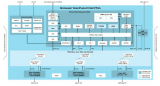
图1.PolarFire FPGA框图
PolarFire FPGA评估板
Microsemi’sPolarFire Evaluation Kit offers high-performance evaluation across a broad class of applications. This kit is ideally suited for high-speed transceiver evaluation, 10Gb Ethernet, IEEE1588, JESD204B, SyncE, CPRI and more. The kit connections include a high pin count (HPC) FPGA mezzanine card (FMC), numerous SMAs, PCIe, Dual Gigabit Ethernet RJ45, SFP+ and USB. A 300K logic element (LE) PolarFire FPGA with DDR4, DDR3 and SPI-flash allow a broad class of high-performance designs to be developed.
PolarFire FPGA评估板硬件特性:
300K LE PolarFire FPGA in an FCG1152 Package (MPF300TS-1FCG1152EES)
HPC FMC Connector
1x SFP+ Cage
IEEE1588 PLL
SMA connectors for testing of full-duplex 12.7Gbps SERDES channel
4GB DDR4 x32 and 2GB DDR3 x16
PCI Express (x4) Edge Connector
2 x RJ45 for 10/100/1000 Ethernet using SGMII on GPIO
Dual 10/100/1000BASE-T PHY (VSC8575) for SyncE and 1588 application
SATA Interface
Power Management Unit for 1 or 1.05v PolarFire FPGA core voltage
USB to UART Interface
Embedded programming and debugging using SPI and JTAG
On-board Power Monitoring
2 x 1Gb SPI Flash Memory
The MicrosemiPolarFire™ FPGA Evaluation Kit (MPF300-EVAL-KIT), which is RoHS-compliant,enables you to evaluate the PolarFire family of FPGAs with support for the following interfaces:
• PCI Express Gen1 and Gen2
• 1 GbE
• DDR3 and DDR4 memory
• FMC HPC with 8 Transceiver lanes
• 1 Full-Duplex Transceiver SMAs
• SFP+ Cage
• UART Interface to FTDI device
• SPI Interface to SPI Flash device
PolarFire FPGA评估板包括:
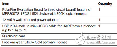
图2.PolarFire FPGA评估板框图
PolarFire FPGA评估板主要特性:
The PolarFire Evaluation Board features the PolarFire MPF300TS-1FCG1152I FPGA. The device hasthe following capabilities:
• 20 Kb dual-port or two-port large static random access memory (LSRAM) block with a built-in singleerror correct double error detect (SECDED)
• 64 × 12 two-port μSRAM block implemented as an array of latches
• 18 × 18 Multiply Accumulate (MACC) block with a pre-adder, a 48-bit accumulator, and an optional16 deep × 18 coefficient RO
• Built-in μPROM, modifiable at program time, readable at run time for user data storage
• Digest integrity check for FPGA, μPROM, and sNVM
• Low-power features:
• Low device static power
• Low inrush current
• Low power transceivers
• Unique Flash*Freeze (F*F) mode
• High-performance communication interfaces
The PolarFire Evaluation Board has several standard interfaces, including:
• VSC8575 with two RJ45 connector for 101001000 Mbps Ethernet
• 8 Full-Duplex Transceiver lanes connected through FMC connector
• FMC HPC connector
• DDR3 memory
• DDR4 memory
• Power Sequence and monitor chip
• x4 Lane PCIe Edge connector
• SFP+ connector
• Two SPI Flash devices
图3.PolarFire FPGA评估板外形图
图4.PolarFire FPGA评估板电路图(1)
图5.PolarFire FPGA评估板电路图(2)
图6.PolarFire FPGA评估板电路图(3)
图7.PolarFire FPGA评估板电路图(4)
图8.PolarFire FPGA评估板电路图(5)
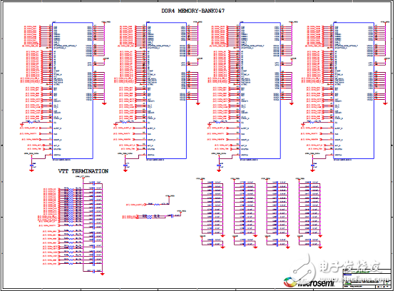
图9.PolarFire FPGA评估板电路图(6)
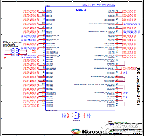
图10.PolarFire FPGA评估板电路图(7)
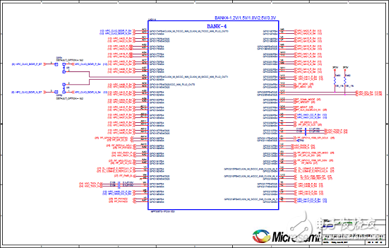
图11.PolarFire FPGA评估板电路图(8)
图12.PolarFire FPGA评估板电路图(9)
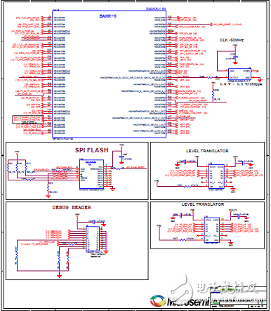
图13.PolarFire FPGA评估板电路图(10)
图14.PolarFire FPGA评估板电路图(11)
图15.PolarFire FPGA评估板电路图(12)
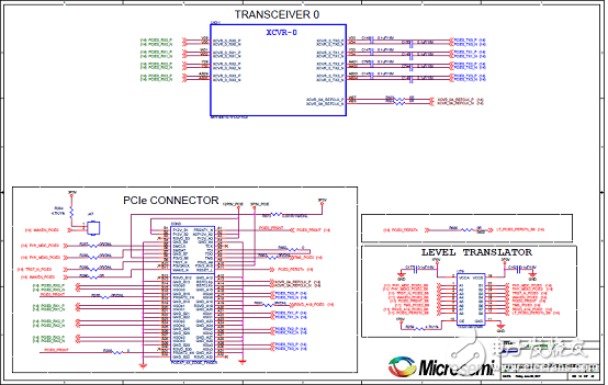
图16.PolarFire FPGA评估板电路图(13)
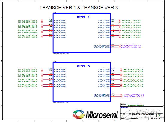
图17.PolarFire FPGA评估板电路图(14)
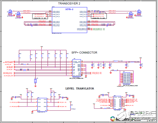
图18.PolarFire FPGA评估板电路图(15)
图19.PolarFire FPGA评估板电路图(16)
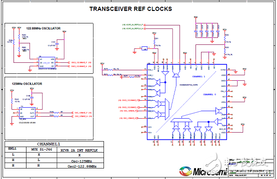
图20.PolarFire FPGA评估板电路图(17)
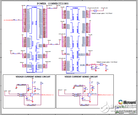
图21.PolarFire FPGA评估板电路图(18)
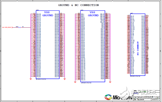
图22.PolarFire FPGA评估板电路图(19)
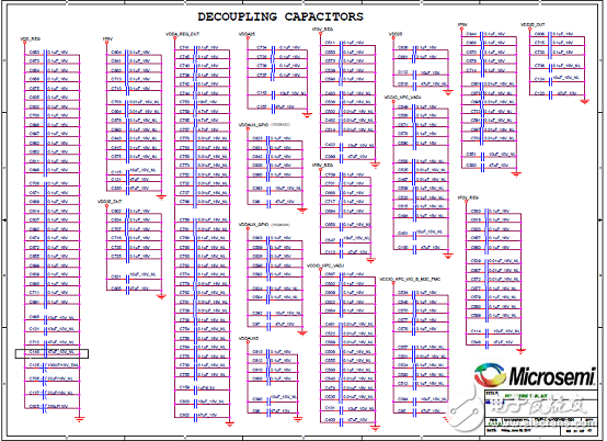
图23.PolarFire FPGA评估板电路图(20)
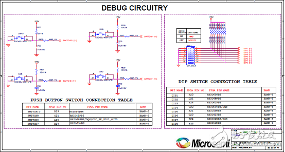
图24.PolarFire FPGA评估板电路图(21)
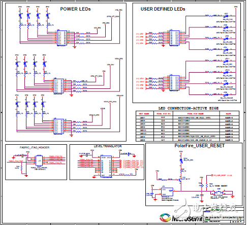
图25.PolarFire FPGA评估板电路图(22)
图26.PolarFire FPGA评估板电路图(23)
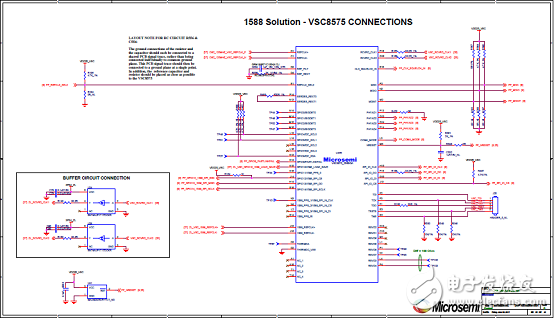
图27.PolarFire FPGA评估板电路图(24)

图28.PolarFire FPGA评估板电路图(25)
图29.PolarFire FPGA评估板电路图(26)
图30.PolarFire FPGA评估板电路图(27)
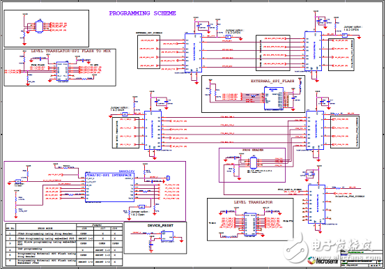
图31.PolarFire FPGA评估板电路图(28)
图32.PolarFire FPGA评估板电路图(29)
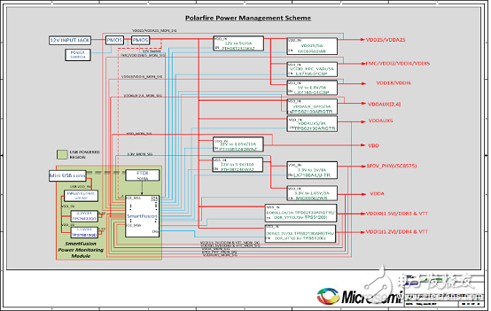
图33.PolarFire FPGA评估板电路图(30)
图34.PolarFire FPGA评估板电路图(31)
图35.PolarFire FPGA评估板电路图(32)
图36.PolarFire FPGA评估板电路图(33)
图37.PolarFire FPGA评估板电路图(34)
图38.PolarFire FPGA评估板电路图(35)
图39.PolarFire FPGA评估板电路图(36)
图40.PolarFire FPGA评估板电路图(37)
图41.PolarFire FPGA评估板电路图(38)
图42.PolarFire FPGA评估板电路图(39)
图43.PolarFire FPGA评估板电路图(40)
图44.PolarFire FPGA评估板电路图(41)
PolarFire FPGA评估板材料元件表:


图45.PolarFire FPGA评估板PCB元件布局图(顶层)

图46.PolarFire FPGA评估板PCB元件布局图(底层)
-
FPGA
+关注
关注
1664文章
22508浏览量
639408
发布评论请先 登录
美高森美的成本优化低功耗中等规模PolarFire FPGA器件 现可与Analog Devices的AD9371 宽带RF收发器互操作
美高森美PolarFire FPGA器件荣获《今日电子》和21ic.com颁发 “2017年度产品奖”
Microsemi PolarFire FPGA视频与成像套件在贸泽开售
超低功耗FPGA解决方案助力机器学习
Microchip发布业界首款基于 RISC-V 指令集架构的 SoC FPGA 开发工具包
首款基于 RISC-V 指令集架构的 SoC FPGA 开发工具包
Microchip FPGA 和基于 SoC 的 RISC-V 生态系统简介
美高森美和Tamba合作开发新型PolarFire器件 提供基于低功耗FPGA的业界领先10G以太网解决方案
Microsemi 基于闪存FPGA架构低功耗SmartFusion2 SoC FPGA开发方案


评论