时序例外约束包括FalsePath、MulticyclePath、MaxDelay、MinDelay。但这还不是最完整的时序约束。
2016-05-29 23:25:10 1424
1424 首先来看带有使能的数据,在本工程中的Tming Report中,也提示了同一个时钟域之间的几个路径建立时间不满足要求
2020-11-14 11:13:126042 
约束流程 说到FPGA时序约束的流程,不同的公司可能有些不一样。反正条条大路通罗马,找到一种适合自己的就行了。从系统上来看,同步时序约束可以分为系统同步与源同步两大类。简单点来说,系统同步是指
2020-11-20 14:44:529155 
时序约束的目的就是告诉工具当前的时序状态,以让工具尽量优化时序并给出详细的分析报告。一般在行为仿真后、综合前即创建基本的时序约束。Vivado使用SDC基础上的XDC脚本以文本形式约束。以下讨论如何进行最基本时序约束相关脚本。
2022-03-11 14:39:1011063 在高速系统中FPGA时序约束不止包括内部时钟约束,还应包括完整的IO时序约束和时序例外约束才能实现PCB板级的时序收敛。因此,FPGA时序约束中IO口时序约束也是一个重点。只有约束正确才能在高速情况下保证FPGA和外部器件通信正确。
2022-09-27 09:56:092392 FPGA开发过程中,离不开时序约束,那么时序约束是什么?简单点说,FPGA芯片中的逻辑电路,从输入到输出所需要的时间,这个时间必须在设定的时钟周期内完成,更详细一点,即需要满足建立和保持时间。
2023-06-06 17:53:071938 
在FPGA设计中,时序约束的设置对于电路性能和可靠性都至关重要。在上一篇的文章中,已经详细介绍了FPGA时序约束的基础知识。
2023-06-06 18:27:1312757 
在FPGA设计中,时序约束对于电路性能和可靠性非常重要。在上一篇的文章中,已经详细介绍了FPGA时序约束的主时钟约束。
2023-06-12 17:29:214234 前面几篇FPGA时序约束进阶篇,介绍了常用主时钟约束、衍生时钟约束、时钟分组约束的设置,接下来介绍一下常用的另外两个时序约束语法“伪路径”和“多周期路径”。
2023-06-12 17:33:533055 时序分析本质上就是一种时序检查,目的是检查设计中所有的D触发器是否能够正常工作,也就是检查D触发器的同步端口(数据输入端口)的变化是否满足建立时间要求(Setup)和保持时间要求(Hold);检查D
2023-07-14 10:48:195776 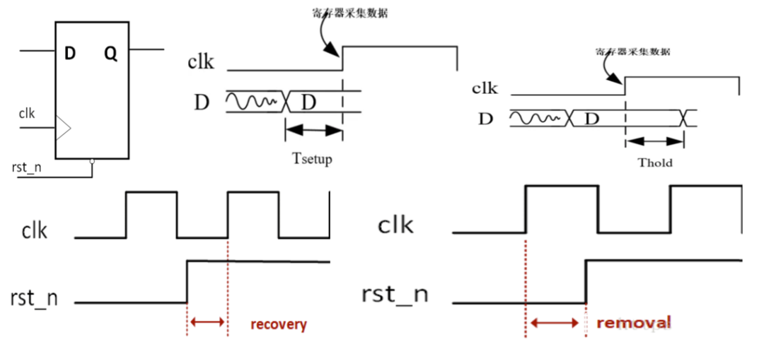
FPGA中时序约束是设计的关键点之一,准确的时钟约束有利于代码功能的完整呈现。进行时序约束,让软件布局布线后的电路能够满足使用的要求。
2023-08-14 17:49:552211 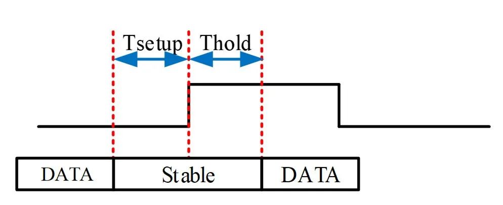
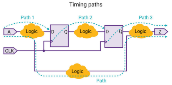
时序路径作为时序约束和时序分析的物理连接关系,可分为片间路径和片内路径。
2023-08-14 17:50:021542 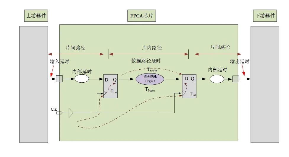
针对第2章节时序路径中用到skew,在本章再仔细讲解一下。
2023-08-14 17:50:582095 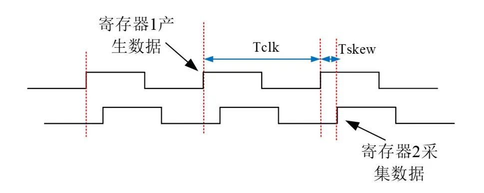
前面讲解了时序约束的理论知识FPGA时序约束理论篇,本章讲解时序约束实际使用。
2023-08-14 18:22:143030 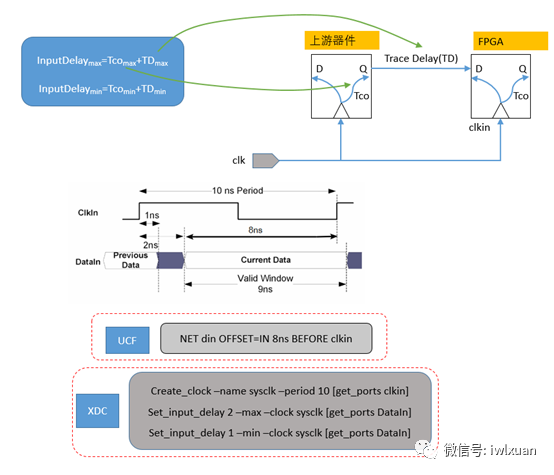
FPGA开发过程中,离不开时序约束,那么时序约束是什么?简单点说,FPGA芯片中的逻辑电路,从输入到输出所需要的时间,这个时间必须在设定的时钟周期内完成,更详细一点,即需要满足建立和保持时间
2023-11-15 17:41:10
FPGA时序约束,总体来分可以分为3类,输入时序约束,输出时序约束,和寄存器到寄存器路径的约束。其中输入时序约束主要指的是从FPGA引脚输入的时钟和输入的数据直接的约束。共分为两大类:1、源同步系统
2015-09-05 21:13:07
刚刚看的一个非常不错的讲解时序约束的资料。在此分享下。
2015-01-21 15:14:35
FalsePath、MulticyclePath、MaxDelay、MinDelay。但这还不是最完整的时序约束。如果仅有这些约束的话,说明设计者的思路还局限在FPGA芯片内部。 2. 核心频率约束
2016-06-02 15:54:04
不是最完整的时序约束。如果仅有这些约束的话,说明设计者的思路还局限在FPGA芯片内部。 2. 核心频率约束+时序例外约束+I/O约束 I/O约束包括引脚分配位置、空闲引脚驱动方式、外部走线延时
2017-12-27 09:15:17
FPGA时序分析与约束(1)本文中时序分析使用的平台:quartusⅡ13.0芯片厂家:Inter1、什么是时序分析?在FPGA中,数据和时钟传输路径是由相应的EDA软件通过针对特定器件的布局布线
2021-07-26 06:56:44
你好: 现在我使用xilinx FPGA进行设计。遇到问题。我不知道FPGA设计是否符合时序要求。我在设计中添加了“时钟”时序约束。我不知道如何添加其他约束。一句话,我不知道哪条路径应该被禁止。我
2019-03-18 13:37:27
FPGA的时序优化高级研修班通知通过设立四大专题,帮助工程师更加深入理解FPGA时序,并掌握时序约束和优化的方法。1.FPGA静态时序分析2.FPGA异步电路处理方法3.FPGA时序约束方法4.FPGA时序优化方法
2013-03-27 15:20:27
FPGA/CPLD的综合、实现过程中指导逻辑的映射和布局布线。下面主要总结一下Xilinx FPGA时序约束设计和分析。
2023-09-21 07:45:57
,因此,为了避免这种情况,必须对fpga资源布局布线进行时序约束以满足设计要求。因为时钟周期是预先知道的,而触发器之间的延时是未知的(两个触发器之间的延时等于一个时钟周期),所以得通过约束来控制触发器之间的延时。当延时小于一个时钟周期的时候,设计的逻辑才能稳定工作,反之,代码会跑飞。
2018-08-29 09:34:47
FPGA静态时序分析——IO口时序(Input Delay /output Delay)1.1概述 在高速系统中FPGA时序约束不止包括内部时钟约束,还应包括完整的IO时序约束和时序例外约束才能
2012-04-25 15:42:03
嗨,大家好,我正在运行smartxplorer ona设计,以获得满足Virtex 6 FPGA时序约束的实现,我看到一些非常奇怪的东西。对于其中一个策略,我得到一个“ -0.440
2018-10-22 10:59:44
《FPGA时序约束与分析》作者特权同学的工程师之道 前些日子,把《最后之舞》的第4集和第10集翻出来再看了一遍,有感于其中的两幕。一幕是公牛在惨败于“坏小子军团”活塞队之后的那个休赛期,没有人
2022-02-07 21:12:38
明德扬时序约束视频简介FPGA时序约束是FPGA设计中的一个重点,也是难点。很多人面对各种时序概念、时序计算公式、时序场景是一头乱麻,望而生畏。现有的教材大部分是介绍概念、时序分析工具和计算公式
2017-06-14 15:42:26
、MulticyclePath、MaxDelay、MinDelay。但这还不是最完整的时序约束。如果仅有这些约束的话,说明设计者的思路还局限在FPGA芯片内部。2. 核心频率约束+时序例外约束+I/O约束 I/O
2017-10-20 13:26:35
1、FPGA中的时序约束--从原理到实例 基本概念 建立时间和保持时间是FPGA时序约束中两个最基本的概念,同样在芯片电路时序分析中也存在。 电路中的建立时间和保持时间其实跟生活中的红绿灯很像
2022-11-15 15:19:27
SDRAM数据手册有如张时序要求图。如何使SDRAM满足时序要求?方法1:添加时序约束。由于Tpcb和时钟频率是固定的,我们可以添加时序约束,让FPGA增加寄存器延时、寄存器到管脚的延时,从而使上述
2016-09-13 21:58:50
本帖最后由 Heracles_月 于 2019-10-30 09:58 编辑
2019-10-30 09:56:55
学习:
学习FPGA的时序约束,理解并掌握时序分析和优化方法。
尝试更复杂的项目,如视频图像处理、网络安全等应用领域中的FPGA应用。
参考实例与社区资源:
研究他人的FPGA实例代码,理解其工作原理
2024-04-28 09:06:45
学习:
学习FPGA的时序约束,理解并掌握时序分析和优化方法。
尝试更复杂的项目,如视频图像处理、网络安全等应用领域中的FPGA应用。
参考实例与社区资源:
研究他人的FPGA实例代码,理解其工作原理
2024-04-28 08:54:35
刚刚开始学习Altera FPGA的时序约束,照着特权同学的一个例子做的 但是出现了下面的问题工程代码:modulequest_test(clk,rst, led);input clk,rst
2014-03-20 12:51:21
Critical Warning: No exact pin location assignment(s) for 77 pins of 80 total pinsInfo: Pin addr_monitor[0] not assigned to an exact location on the deviceInfo: Pin addr_monitor[2] not assigned to an exact location on the deviceInfo: Pin addr_monitor[4] not assigned to an exact location on the deviceInfo: Pin addr_monitor[6] not assigned to an exact location on the deviceInfo: Pin addr_monitor[8] not assigned to an exact location on the deviceInfo: Pin addr_monitor[10] not assigned to an exact location on the deviceInfo: Pin addr_monitor[12] not assigned to an exact location on the deviceInfo: Pin data_out[0] not assigned to an exact location on the deviceInfo: Pin data_out[2] not assigned to an exact location on the deviceInfo: Pin data_out[4] not assigned to an exact location on the deviceInfo: Pin data_out[6] not assigned to an exact location on the deviceInfo: Pin max[0] not assigned to an exact location on the deviceInfo: Pin max[2] not assigned to an exact location on the deviceInfo: Pin max[4] not assigned to an exact location on the deviceInfo: Pin max[6] not assigned to an exact location on the deviceInfo: Pin max[8] not assigned to an exact location on the deviceInfo: Pin max[10] not assigned to an exact location on the deviceInfo: Pin max[12] not assigned to an exact location on the deviceInfo: Pin max[14] not assigned to an exact location on the deviceInfo: Pin max[16] not assigned to an exact location on the deviceInfo: Pin max[18] not assigned to an exact location on the deviceInfo: Pin max[20] not assigned to an exact location on the deviceInfo: Pin max[22] not assigned to an exact location on the deviceInfo: Pin max[24] not assigned to an exact location on the deviceInfo: Pin max[26] not assigned to an exact location on the deviceInfo: Pin max[28] not assigned to an exact location on the deviceInfo: Pin max[30] not assigned to an exact location on the deviceInfo: Pin max[32] not assigned to an exact location on the deviceInfo: Pin max[34] not assigned to an exact location on the deviceInfo: Pin max[36] not assigned to an exact location on the deviceInfo: Pin max[38] not assigned to an exact location on the deviceInfo: Pin max[40] not assigned to an exact location on the deviceInfo: Pin max[42] not assigned to an exact location on the deviceInfo: Pin max[44] not assigned to an exact location on the deviceInfo: Pin max[46] not assigned to an exact location on the deviceInfo: Pin max[48] not assigned to an exact location on the deviceInfo: Pin max[50] not assigned to an exact location on the deviceInfo: Pin QUAN_SIG[0] not assigned to an exact location on the deviceInfo: Pin stat_finish not assigned to an exact location on the deviceInfo: Pin addr_monitor[1] not assigned to an exact location on the deviceInfo: Pin addr_monitor[3] not assigned to an exact location on the deviceInfo: Pin addr_monitor[5] not assigned to an exact location on the deviceInfo: Pin addr_monitor[7] not assigned to an exact location on the deviceInfo: Pin addr_monitor[9] not assigned to an exact location on the deviceInfo: Pin addr_monitor[11] not assigned to an exact location on the deviceInfo: Pin addr_monitor[13] not assigned to an exact location on the deviceInfo: Pin data_out[1] not assigned to an exact location on the deviceInfo: Pin data_out[3] not assigned to an exact location on the deviceInfo: Pin data_out[5] not assigned to an exact location on the deviceInfo: Pin data_out[7] not assigned to an exact location on the deviceInfo: Pin max[1] not assigned to an exact location on the deviceInfo: Pin max[3] not assigned to an exact location on the deviceInfo: Pin max[5] not assigned to an exact location on the deviceInfo: Pin max[7] not assigned to an exact location on the deviceInfo: Pin max[9] not assigned to an exact location on the deviceInfo: Pin max[11] not assigned to an exact location on the deviceInfo: Pin max[13] not assigned to an exact location on the deviceInfo: Pin max[15] not assigned to an exact location on the deviceInfo: Pin max[17] not assigned to an exact location on the deviceInfo: Pin max[19] not assigned to an exact location on the deviceInfo: Pin max[21] not assigned to an exact location on the deviceInfo: Pin max[23] not assigned to an exact location on the deviceInfo: Pin max[25] not assigned to an exact location on the deviceInfo: Pin max[27] not assigned to an exact location on the deviceInfo: Pin max[29] not assigned to an exact location on the deviceInfo: Pin max[31] not assigned to an exact location on the deviceInfo: Pin max[33] not assigned to an exact location on the deviceInfo: Pin max[35] not assigned to an exact location on the deviceInfo: Pin max[37] not assigned to an exact location on the deviceInfo: Pin max[39] not assigned to an exact location on the deviceInfo: Pin max[41] not assigned to an exact location on the deviceInfo: Pin max[43] not assigned to an exact location on the deviceInfo: Pin max[45] not assigned to an exact location on the deviceInfo: Pin max[47] not assigned to an exact location on the deviceInfo: Pin max[49] not assigned to an exact location on the deviceInfo: Pin max[51] not assigned to an exact location on the deviceInfo: Pin QUAN_SIG[1] not assigned to an exact location on the deviceCritical Warning: From pll_20MHz_inst|altpll_component|auto_generated|pll1|clk[0] (Rise) to pll_20MHz_inst|altpll_component|auto_generated|pll1|clk[0] (Rise) (setup and hold)Critical Warning: From pll_20MHz_inst|altpll_component|auto_generated|pll1|clk[1] (Rise) to pll_20MHz_inst|altpll_component|auto_generated|pll1|clk[0] (Rise) (setup and hold)Critical Warning: From pll_20MHz_inst|altpll_component|auto_generated|pll1|clk[0] (Rise) to pll_20MHz_inst|altpll_component|auto_generated|pll1|clk[1] (Rise) (setup and hold)Critical Warning: The following clock transfers have no clock uncertainty assignment. For more accurate results, apply clock uncertainty assignments or use the derive_clock_uncertainty command.Critical Warning: From pll_20MHz_inst|altpll_component|auto_generated|pll1|clk[0] (Fall) to pll_20MHz_inst|altpll_component|auto_generated|pll1|clk[0] (Rise) (setup and hold)Critical Warning: From pll_20MHz_inst|altpll_component|auto_generated|pll1|clk[1] (Fall) to pll_20MHz_inst|altpll_component|auto_generated|pll1|clk[0] (Rise) (setup and hold)Critical Warning: From pll_20MHz_inst|altpll_component|auto_generated|pll1|clk[1] (Rise) to pll_20MHz_inst|altpll_component|auto_generated|pll1|clk[1] (Rise) (setup and hold)Critical Warning: From pll_20MHz_inst|altpll_component|auto_generated|pll1|clk[0] (Fall) to pll_20MHz_inst|altpll_component|auto_generated|pll1|clk[0] (Rise) (setup and hold)Critical Warning: From pll_20MHz_inst|altpll_component|auto_generated|pll1|clk[1] (Fall) to pll_20MHz_inst|altpll_component|auto_generated|pll1|clk[0] (Rise) (setup and hold)Critical Warning: From pll_20MHz_inst|altpll_component|auto_generated|pll1|clk[1] (Rise) to pll_20MHz_inst|altpll_component|auto_generated|pll1|clk[1] (Rise) (setup and hold)Critical Warning: The following clock transfers have no clock uncertainty assignment. For more accurate results, apply clock uncertainty assignments or use the derive_clock_uncertainty command.Critical Warning: From pll_20MHz_inst|altpll_component|auto_generated|pll1|clk[0] (Fall) to pll_20MHz_inst|altpll_component|auto_generated|pll1|clk[0] (Rise) (setup and hold)Critical Warning: From pll_20MHz_inst|altpll_component|auto_generated|pll1|clk[1] (Fall) to pll_20MHz_inst|altpll_component|auto_generated|pll1|clk[0] (Rise) (setup and hold)Critical Warning: From pll_20MHz_inst|altpll_component|auto_generated|pll1|clk[1] (Rise) to pll_20MHz_inst|altpll_component|auto_generated|pll1|clk[1] (Rise) (setup and hold)Critical Warning: From pll_20MHz_inst|altpll_component|auto_generated|pll1|clk[0] (Fall) to pll_20MHz_inst|altpll_component|auto_generated|pll1|clk[0] (Rise) (setup and hold)Critical Warning: From pll_20MHz_inst|altpll_component|auto_generated|pll1|clk[1] (Fall) to pll_20MHz_inst|altpll_component|auto_generated|pll1|clk[0] (Rise) (setup and hold)Critical Warning: From pll_20MHz_inst|altpll_component|auto_generated|pll1|clk[1] (Rise) to pll_20MHz_inst|altpll_component|auto_generated|pll1|clk[1] (Rise) (setup and hold)Critical Warning: The following clock transfers have no clock uncertainty assignment. For more accurate results, apply clock uncertainty assignments or use the derive_clock_uncertainty command.Critical Warning: From pll_20MHz_inst|altpll_component|auto_generated|pll1|clk[0] (Fall) to pll_20MHz_inst|altpll_component|auto_generated|pll1|clk[0] (Rise) (setup and hold)Critical Warning: From pll_20MHz_inst|altpll_component|auto_generated|pll1|clk[1] (Fall) to pll_20MHz_inst|altpll_component|auto_generated|pll1|clk[0] (Rise) (setup and hold)Critical Warning: From pll_20MHz_inst|altpll_component|auto_generated|pll1|clk[1] (Rise) to pll_20MHz_inst|altpll_component|auto_generated|pll1|clk[1] (Rise) (setup and hold)Critical Warning: From pll_20MHz_inst|altpll_component|auto_generated|pll1|clk[0] (Fall) to pll_20MHz_inst|altpll_component|auto_generated|pll1|clk[0] (Rise) (setup and hold)Critical Warning: From pll_20MHz_inst|altpll_component|auto_generated|pll1|clk[1] (Fall) to pll_20MHz_inst|altpll_component|auto_generated|pll1|clk[0] (Rise) (setup and hold)Critical Warning: From pll_20MHz_inst|altpll_component|auto_generated|pll1|clk[1] (Rise) to pll_20MHz_inst|altpll_component|auto_generated|pll1|clk[1] (Rise) (setup and hold)Critical Warning: Timing requirements not met
2020-04-29 16:23:29
我是一个FPGA初学者,关于时序约束一直不是很明白,时序约束有什么用呢?我只会全局时钟的时序约束,如何进行其他时序约束呢?时序约束分为哪几类呢?不同时序约束的目的?
2012-07-04 09:45:37
时序约束与时序分析 ppt教程
本章概要:时序约束与时序分析基础常用时序概念QuartusII中的时序分析报告
设置时序约束全局时序约束个别时
2010-05-17 16:08:02 0
0 时序约束用户指南包含以下章节: ?第一章“时序约束用户指南引言” ?第2章“时序约束的方法” ?第3章“时间约束原则” ?第4章“XST中指定的时序约束” ?第5章“Synplify中指定的时
2010-11-02 10:20:560 FPGA时序约束方法很好地资料,两大主流的时序约束都讲了!
2015-12-14 14:21:2519 赛灵思FPGA设计时序约束指南,下来看看
2016-05-11 11:30:1949 FPGA学习资料教程之Xilinx时序约束培训教材
2016-09-01 15:27:270 电子专业,单片机、DSP、ARM相关知识学习资料与教材
2016-10-26 17:40:280 时序约束可以使得布线的成功率的提高,减少ISE布局布线时间。这时候用到的全局约束就有周期约束和偏移约束。周期约束就是根据时钟频率的不同划分为不同的时钟域,添加各自周期约束。对于模块的输入输出端口添加
2017-02-09 02:56:06918 Xilinx FPGA编程技巧常用时序约束介绍,具体的跟随小编一起来了解一下。
2018-07-14 07:18:005223 
作时序和布局约束是实现设计要求的关键因素。本文是介绍其使用方法的入门读物。 完成 RTL 设计只是 FPGA 设计量产准备工作中的一部分。接下来的挑战是确保设计满足芯片内的时序和性能要求。为此,您
2017-11-17 05:23:013260 
一个好的FPGA设计一定是包含两个层面:良好的代码风格和合理的约束。时序约束作为FPGA设计中不可或缺的一部分,已发挥着越来越重要的作用。毋庸置疑,时序约束的最终目的是实现时序收敛。时序收敛作为
2017-11-17 07:54:362967 
针对八通道采样器AD9252的高速串行数据接口的特点,提出了一种基于FPGA时序约束 的高速解串方法。使用Xilinx公司的FPGA接收高速串行数据,利用FPGA内部的时钟管理模块DCM、位置约束
2017-11-17 12:27:017352 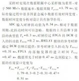
作为赛灵思用户论坛的定期访客(见 ),我注意到新用户往往对时序收敛以及如何使用时序约束来达到时序收敛感到困惑。为帮助 FPGA设计新手实现时序收敛,让我们来深入了解时序约束以及如何利用时序约束实现
2017-11-24 19:37:555955 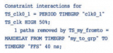
在简单电路中,当频率较低时,数字信号的边沿时间可以忽略时,无需考虑时序约束。但在复杂电路中,为了减少系统中各部分延时,使系统协同工作,提高运行频率,需要进行时序约束。通常当频率高于50MHz时,需要考虑时序约束。
2018-03-30 13:42:5915212 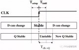
介绍FPGA约束原理,理解约束的目的为设计服务,是为了保证设计满足时序要求,指导FPGA工具进行综合和实现,约束是Vivado等工具努力实现的目标。所以首先要设计合理,才可能满足约束,约束反过来检查
2018-06-25 09:14:007199 从最近一段时间工作和学习的成果中,我总结了如下几种进行时序约束的方法。按照从易到难的顺序排列如下:
2018-08-07 14:14:0014317 
FPGA中的时序问题是一个比较重要的问题,时序违例,尤其喜欢在资源利用率较高、时钟频率较高或者是位宽较宽的情况下出现。建立时间和保持时间是FPGA时序约束中两个最基本的概念,同样在芯片电路时序分析中也存在。
2019-12-23 07:02:004742 
FPGA中的时序问题是一个比较重要的问题,时序违例,尤其喜欢在资源利用率较高、时钟频率较高或者是位宽较宽的情况下出现。建立时间和保持时间是FPGA时序约束中两个最基本的概念,同样在芯片电路时序分析中也存在。
2019-12-23 07:01:002671 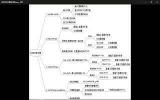
/FPGA的内部结构、设计流程和开发工具,详细论述了CPLD/FPGA设计的时序约束、仿真验证和综合实现,重点介绍了嵌入PowerPC405的平台FPGA开发以及FPGA在数字信号处理领域的最新应用。
2019-09-05 08:00:0022 FPGA在与外部器件打交道时,端口如果为输入则与input delay约束相关,如果最为输出则output delay,这两种约束的值究竟是什么涵义,在下文中我也会重点刨析,但是前提是需要理解图1和图2建立余量和保持余量。
2019-11-10 10:06:235266 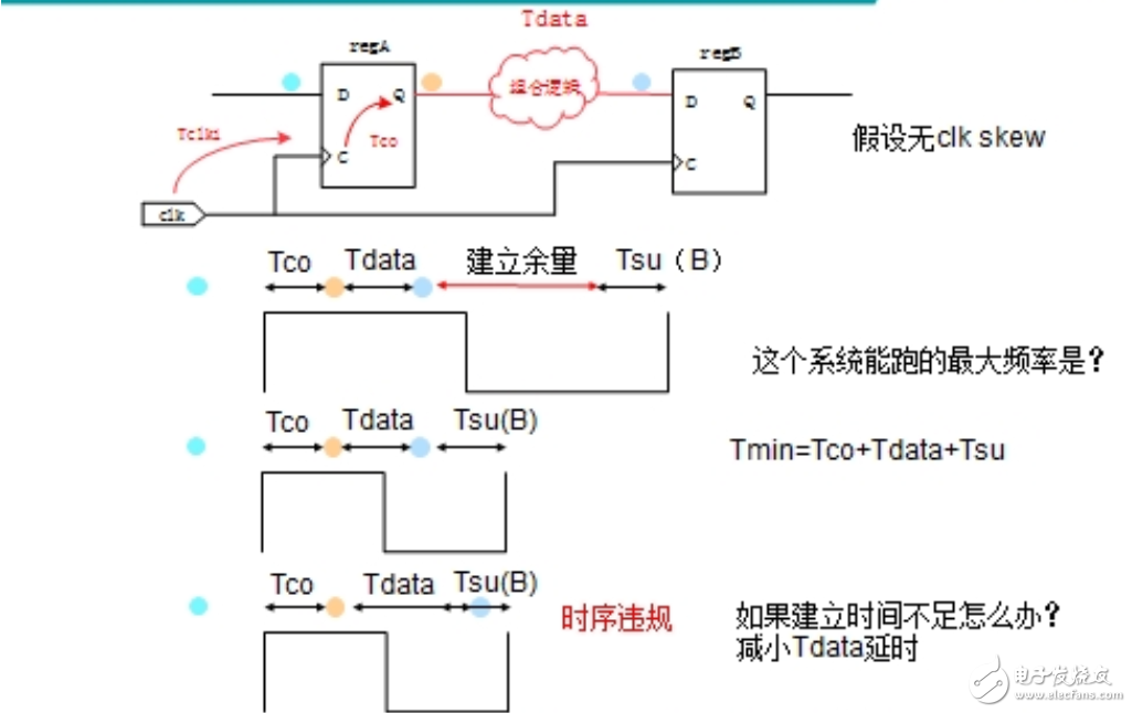
首先来看什么是时序约束,泛泛来说,就是我们告诉软件(Vivado、ISE等)从哪个pin输入信号,输入信号要延迟多长时间,时钟周期是多少,让软件PAR(Place and Route)后的电路能够
2020-01-28 17:34:004750 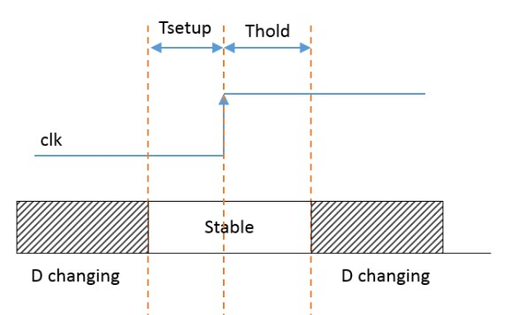
典型的时序路径有4类,如下图所示,这4类路径可分为片间路径(标记①和标记③)和片内路径(标记②和标记④)。
2020-01-27 10:37:003235 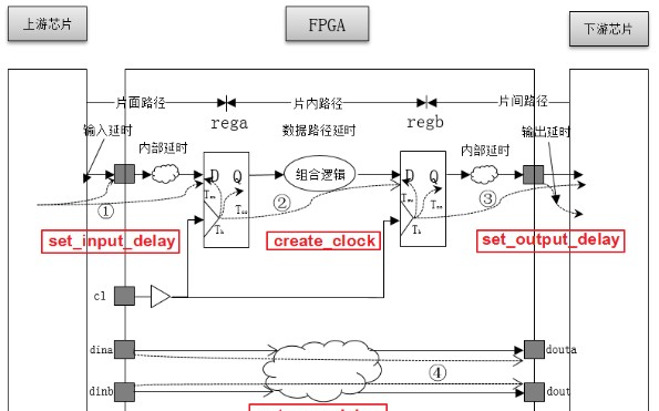
伪路径约束 在本章节的2 约束主时钟一节中,我们看到在不加时序约束时,Timing Report会提示很多的error,其中就有跨时钟域的error,我们可以直接在上面右键,然后设置两个时钟的伪路径
2020-11-14 11:28:103628 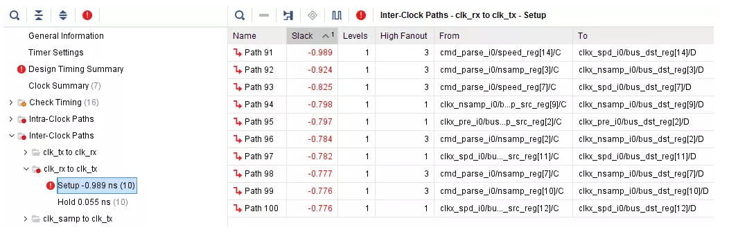
时序分析结果,并根据设计者的修复使设计完全满足时序约束的要求。本章包括以下几个部分: 1.1 静态时序分析简介 1.2 FPGA 设计流程 1.3 TimeQuest 的使用 1.4 常用时序约束 1.5 时序分析的基本概念
2020-11-11 08:00:0067 下面举一个最简单的例子来说明时序分析的基本概念。假设信号需要从输入到输出在FPGA内部经过一些逻辑延时和路径延时。我们的系统要求这个信号在FPGA内部的延时不能超过15ns,而开发工具在执行过程中
2021-01-11 17:44:438 对自己的设计的实现方式越了解,对自己的设计的时序要求越了解,对目标器件的资源分布和结构越了解,对EDA工具执行约束的效果越了解,那么对设计的时序约束目标就会越清晰,相应地,设计的时序收敛过程就会更可控。
2021-01-11 17:44:448 说到FPGA时序约束的流程,不同的公司可能有些不一样。反正条条大路通罗马,找到一种适合自己的就行了。从系统上来看,同步时序约束可以分为系统同步与源同步两大类。简单点来说,系统同步是指FPGA与外部
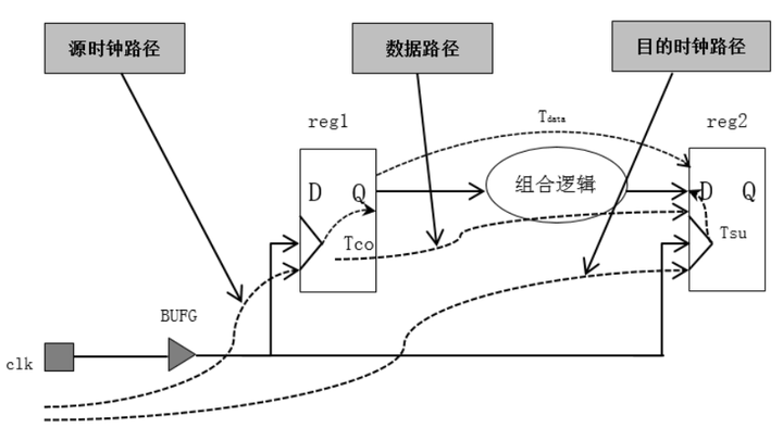
2021-01-11 17:46:3214 组合逻辑延迟和走线延迟。Tsu表示捕获寄存器建立时间要求。Th表示捕获寄存器保持时间要求。其中Tco、Tsu和Th是由FPGA的芯片工艺决定的。所以,我们所谓的时序约束,实际上就是对时钟延迟和Tdata做一定的要求或者干预,其中Tdata由组合逻辑(代码)及布局布线决定,这也决
2021-01-12 17:31:369 在FPGA 设计中,很少进行细致全面的时序约束和分析,Fmax是最常见也往往是一个设计唯一的约束。这一方面是由FPGA的特殊结构决定的,另一方面也是由于缺乏好用的工具造成的。好的时序约束可以指导布局布线工具进行权衡,获得最优的器件性能,使设计代码最大可能的反映设计者的设计意图。
2021-01-12 17:31:008 xilinx的Vivado工具也一直在更新,到本人记录此文的时候,Vivado已经有2017.3版本了,建议大家使用最新的Vivado工具。
2021-01-12 17:31:5310 举个形象的比喻:就好比我要让代工厂(类比quartus ii)给我加工一批零件,要求长宽高为10x10x10cm,误差不超过1mm(类比时序约束条件)。代工厂按要求(即约束条件)开始进行生产加工
2021-01-13 16:02:008 由于每次我都写了功能仿真过后,放到门级仿真,就出问题,而门级仿真通常对实际还是有一定的指导意义的,通常我只要门级仿真跑不出来,多半实际都没跑出来,而且门级仿真调试起来相当麻烦,所以功能仿真+时序约束+signal tap 才是最好的方法。
2021-01-13 16:02:168 首先,我们点进去都会叫我们选择一个模型,来建立网表,如果,我们选择slow,那么我们知道对setup slack自然会有影响更大,如果我们选择fast模型,就会对hold slack的模型影响更大。
2021-01-13 16:02:009 本篇文章用于总结之前学习的time quest,并且我已经能够利用公式,计算出slack了,并能够根据setup slack来更改优化代码了。时光由隔了1个月,时序分析的路没有终点,本篇文章是对之前
2021-01-13 16:02:0010 在高速系统中FPGA时序约束不止包括内部时钟约束,还应包括完整的IO时序约束利序例外约束才能实现PCB板级的时序收敛。因此,FPGA时序约束中IO口时序约束也是重点。只有约東正确才能在高速情况下保证FPGA和外部器件通信正确
2021-01-13 17:13:0011 一、前言 无论是FPGA应用开发还是数字IC设计,时序约束和静态时序分析(STA)都是十分重要的设计环节。在FPGA设计中,可以在综合后和实现后进行STA来查看设计是否能满足时序上的要求。
2021-08-10 09:33:106579 
A 时序约束的概念和基本策略 时序约束主要包括周期约束(FFS到FFS,即触发器到触发器)和偏移约束(IPAD到FFS、FFS到OPAD)以及静态路径约束(IPAD到OPAD)等3种。通过附加
2021-09-30 15:17:465927 A 时序约束的概念和基本策略 时序约束主要包括周期约束(FFS到FFS,即触发器到触发器)和偏移约束(IPAD到FFS、FFS到OPAD)以及静态路径约束(IPAD到OPAD)等3种。通过附加
2021-10-11 10:23:096573 
本文章探讨一下FPGA的时序约束步骤,本文章内容,来源于配置的明德扬时序约束专题课视频。
2022-03-16 09:17:194001 
上一篇《FPGA时序约束分享01_约束四大步骤》一文中,介绍了时序约束的四大步骤。
2022-03-18 10:29:282166 
本文章探讨一下FPGA的时序input delay约束,本文章内容,来源于配置的明德扬时序约束专题课视频。
2022-05-11 10:07:564989 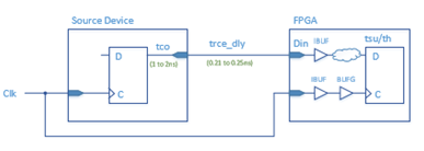
很多读者对于怎么进行约束,约束的步骤过程有哪些等,不是很清楚。明德扬根据以往项目的经验,把时序约束的步骤,概括分成四大步
2022-07-02 10:56:456314 
明德扬有完整的时序约束课程与理论,接下来我们会一章一章以图文结合的形式与大家分享时序约束的知识。要掌握FPGA时序约束,了解D触发器以及FPGA运行原理是必备的前提。今天第一章,我们就从D触发器开始讲起。
2022-07-11 11:33:106143 
本文章探讨一下FPGA的时序input delay约束,本文章内容,来源于明德扬时序约束专题课视频。
2022-07-25 15:37:073757 
时间裕量包括建立时间裕量和保持时间裕量(setup slack和hold slack)。从字面上理解,所谓“裕量”即富余的、多出的。什么意思呢?即保持最低要求的建立时间或保持时间所多出的时间,那么“裕量”越多,意味着时序约束越宽松。
2022-08-04 17:45:041079 时间裕量包括建立时间裕量和保持时间裕量(setup slack和hold slack)。从字面上理解,所谓“裕量”即富余的、多出的。
2023-02-06 11:06:03793 1、时序错误的影响 一个设计的时序报告中,design run 时序有红色,裕量(slack)为负数时,表示时序约束出现违例,虽然个别违例不代表你的工程就有致命的问题,但是这是一
2023-03-17 03:25:032014 FPGA/CPLD的综合、实现过程中指导逻辑的映射和布局布线。下面主要总结一下Xilinx FPGA时序约束设计和分析。
2023-04-27 10:08:222404 前面几篇文章已经详细介绍了FPGA时序约束基础知识以及常用的时序约束命令,相信大家已经基本掌握了时序约束的方法。
2023-06-23 17:44:004086 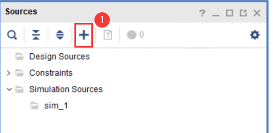
STA(Static Timing Analysis,即静态时序分析)在实际FPGA设计过程中的重要性是不言而喻的
2023-06-26 09:01:531276 
典型的时序路径有4类,如下图所示,这4类路径可分为片间路径(标记①和标记③)和片内路径(标记②和标记④)。
2023-06-26 10:30:431138 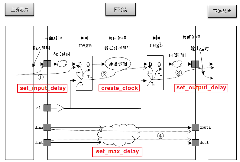
FPGA开发过程中软件的综合布线耗时很长,这块对FPGA产品开发的进度影响很大。
2023-06-26 14:58:091498 
现有一块ADC连接到FPGA上,需要在FPGA上实现高速数据的读取,那么第一步自然就是完成可靠的硬件连线
2023-06-28 09:07:381308 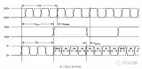
本文主要介绍了时序设计和时序约束。
2023-07-04 14:43:522391 建立时间和保持时间是FPGA时序约束中两个最基本的概念,同样在芯片电路时序分析中也存在。
2024-08-06 11:40:182366 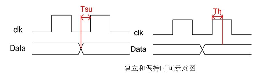
Vivado中时序分析工具默认会分析设计中所有时钟相关的时序路径,除非时序约束中设置了时钟组或false路径。使用set_clock_groups命令可以使时序分析工具不分析时钟组中时钟的时序路径,使用set_false_path约束则会双向忽略时钟间的时序路径
2025-04-23 09:50:281079 
 电子发烧友App


 工商网监
工商网监
评论