 应用指导 | CGAN003: GaN switching behavior analysis

众所周知,GaN 功率器件具有传统功率器件无可比拟的性能优势,如大幅提升的开关速度和显著降低的开关损耗,从而提供更优的整体效率,这使得GaN器件在高频、高效率的应用中展现出明显优势。我们的应用指导将帮助客户更好得使用云镓的 GaN 器件,更大限度去挖掘云镓的 GaN 器件的能力。本次发布云镓应用手册第三弹: GaN switching behavior analysis。此外,客户可以通过云镓半导体官方网站或者微信公众号了解到更多云镓 GaN 产品资讯和相关技术文档。
Part 1 : Overview ofDPT
01
Why do we need DPT to measure GaN?
Whydo we need double pulse tester to measure GaN FETs?
Extracting switching parameters (ton, toff, tr, tf)
Extractingswitching loss (Eon, Eoff)
Emulatingsystem behavior, e.g. turn-off drain spike, switching time and etc.
Evaluating dynamic performance, e.g. dynamic Ron, D-HTOL, switching SOA, and etc.
Noneed of high-power equipment, low-cost scheme

02
An example of DPT-650V/30mΩ CloudSemi GaN

01
1stpulse turn-on: zero-current switching

Stageof start-up,zero-currentturn-on (capacitive-load switching):
- Vdsof rectifier GaN:Vbus→ 0; Vdsof synchronous GaN: 0 → Vbus
- Thesetup can be treated as a capacitive-load switching:
- Oscilloscope-captured Ids comes from charging Coss of Syn GaN: Ids = C(Vbus-Vds)*dv/dt
- DischargingCossof Rec GaN cannot be directlycaptured by oscilloscope: ICoss= Coss*dv/dt
- Current through Rec GaN channel: Ich, rec = Ids + Coss*dv/dt
02
HSW turn-on transient: Vgoff to Vth
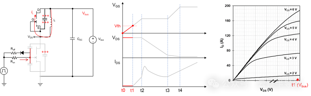
t0~t1,gate drive charges Ciss of Rec GaN:
Vgsof Rec GaN rises to Vth. No current flowsthrough RecGaN.
Loadcurrent flows through inductor and Syn GaN.
UntilVgsof Rec GaN reach to its Vth, loadcurrent starts to commutate and flow through it.
03
HSW turn-on transient: current commutation

t1~t2,current commutation:
AsVgsof Rec GaN reaches Vth,current starts to flow through Rec GaN. Load current gradually commutates fromSyn GaN to Rec GaN, as Vgsincreases;
Duringcurrent commutation, the gate driver charges Ciss until Rec GaN has currentcapability of IL.[Ids|(Vgs=Vgp) = IL]
WhenVgs= Vgp (Miller plateau, = Vth + IL/gm),all the inductive-load current flows through the Rec GaN.
Inthis duration, Rec GaN Idsoverlaps with Vds, andI-Voverlap lossdominates and can be calculated by integrating I&V.
04
HSW turn-on transient: voltage commutation

t2~t3,voltage commutation:
AsVgsof Rec GaN reaches Vgp, allthe load current flows through Rec GaN;
Then,RecGaN Cossstarts to discharge from Vbusto Von& SynGaN Cossstarts to charge to Vbus
RecGaN Cossdischarging cannot be captured,but SynGaN Cosscharging can be recognized from Ids waveform
Duringthis duration, the loss on Rec GaN consists of 2main parts:
I-V overlap loss
Cap loss fromSyn/Rec GaN: Vbus*Qoss

GaN features much lower Qossandswitching loss Psw comparing to Si SJ
05
HSW turn-on transient: gate over-drive

t3~t4,gate over-drive to make GaN fully turn-on:
Gatedriver continue to charge Ciss fromVgp to Vdrive (e.g. 6V), making GaN FET fullyturn-on
Von= IL* Rdson (Vgs= Vdrive). Therecommended gate drive voltage for CloudSemi E-mode GaNis ~6.0V.
Aftert4, inductive load will continue to excite, following dIL = Vbus/L * dt
Conductionloss on Rec GaN FET dominates in this duration
Comparing to Si SJ, GaN FET features much lower gate charge QG

06
Turn-on period: excitation

t4~t5,inductive load excitation:
dIL = Vbus/L *dt, Ids = IL
Cissstops charging
Currentflowingthrough GaN channel gradually increases
RecGaN FET works in linear region.
Conductionloss on Rec GaN FET dominates in this duration
07
HSW turn-off transient: VGS → Vgp

t5~t6, Ciss starts discharging:
Rec GaN Ciss starts to discharge, until GaN enters saturation mode (Vgs= Vgp, Idsat = IL).
Here,Vgp =Vth + IL/gm
RecGaN works from linear region to saturation region
Conductionloss on Rec GaN FET dominates in this duration
08
HSW turn-off transient: voltage commutation

t6~t7,voltage commutation (Rec GaN Vdsrises to Vbus):
Loadcurrent charges the switching node (charging CossofRec GaN, discharging Cossof Syn GaN)
Parameterof Qossis crucial, and determinescharging/discharging speed (i.e. switching speed)
Powerloss on Rec GaN mainly comes from I-V overlap loss
09
HSW turn-off transient: current commutation

t7~t8,current commutation:
Load current gradually commutates from Rec GaN to Syn GaN, as Vgsdecreases;
Duringcurrent commutation, the gate driver discharges Ciss until Rec GaN has been turned off(Vgs= Vth)
WhenRec GaN Vgs= Vth (i.e. after t8), all the inductive-load current flows through theSyn GaN.
Powerloss mainly comes from I-V overlap loss
Part 3 : Summary
01
Summary


更多关于 GaN 器件在系统中的损耗,我们将以 200V→400V 同步 boost 和 48V→12V同步 buck 来进行实例说明,敬请期待。
-
半导体
+关注
关注
339文章
31248浏览量
266601 -
功率器件
+关注
关注
43文章
2222浏览量
95479 -
GaN
+关注
关注
21文章
2385浏览量
84486
发布评论请先 登录
(开关电源EMI设计)Integrated EMI/Thermal Design for Switching Power Supplies
switching power supply (SMPS)开关频率
undefined behavior
源代码在STM8S003F3P6微控制器中损坏
A finite element analysis of f
Analysis of dv/dt Induced Spur
Circuit Analysis II with MATLA

Effects of High Switching Freq
Monitoring and Analysis-PQ Aud
什么是CS (Circuit Switching)
Stability Analysis of Current Fe
Optimization of Extraction Technology and Property Analysis of CORTEX
应用指导 | CGAN002: How to read GaN datasheet

应用指导 | CGAN005: GaN FET SPICE model simulation
应用指导 | CGAN004: GaN FET loss calculation (Boost converter)


评论