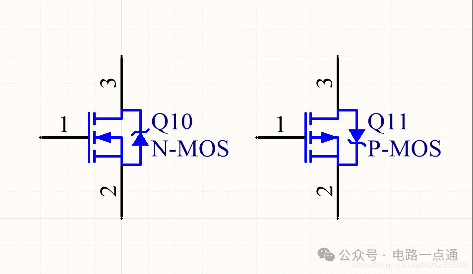
 N-MOS工艺芯片与P-MOS工艺芯片对比

一、How does Over Current Protection (OCP)work?
When over-current protection (OCP) is enabled, the power system turns off the output if the output current reaches the current limit setting and transitions from constant voltage (CV) operation to constant current (CC) operation.
With OCP turned on, the OCP takes over after a specified time delay and shuts down the output of the power supply. The delay time is programmable. This prevents OCP from shutting down the DC power supply from short current spikes and other acceptably short overloads that are not considered harmful. In comparison, with Over Voltage Protection (OVP), the output is disabled immediately. OVP is usually always enabled and cannot be turned off. However, unlike OVP, OCP can be turned on and off and its default is usually off. A typical OCP event is illustrated here:
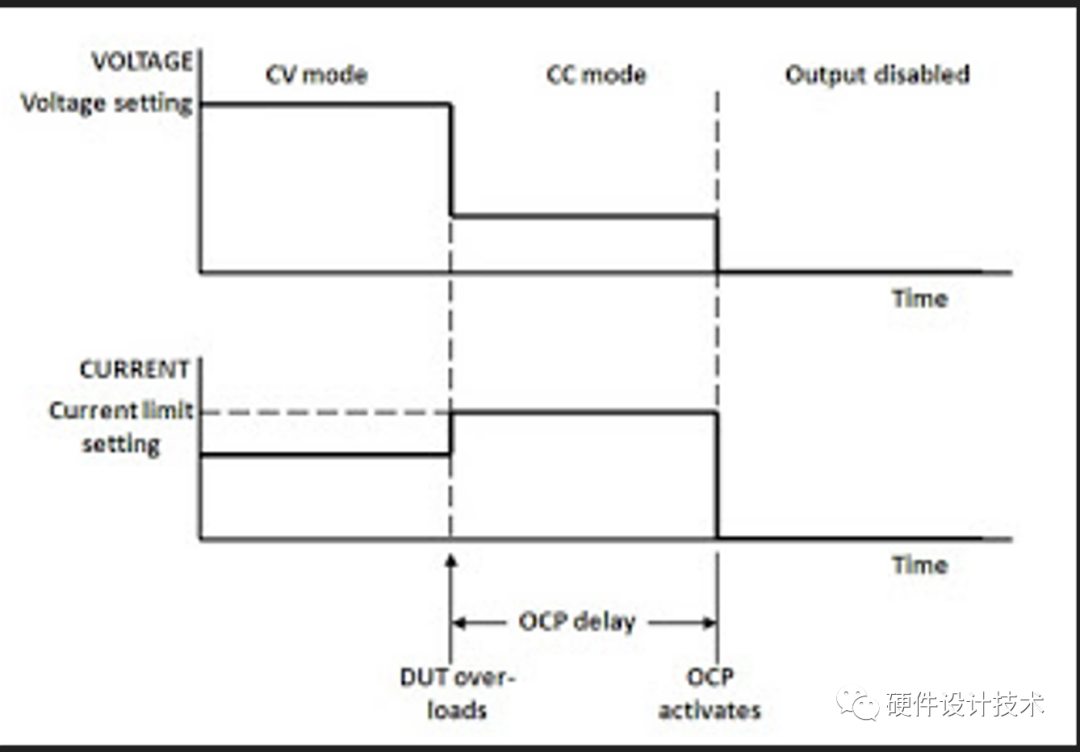
Wecan specify an OCP delay to prevent momentary output settings, load, and status changes from tripping the over-current protection. In most cases these momentary conditions would not be considered an over-current protection fault, and having an OCP condition disable the output when they occur would be a nuisance. Specifying an OCP delay lets the OCP circuit ignore these momentary changes during the specified delay period. Once the OCP delay time has expired and the over-current condition persists, the output will shut down. Other factors include the difference between old output value and new output value, the current limit setting, and the load capacitance in CV operation or load inductance in CC operation. The delay required must be determined experimentally on a case-by-case basis.
二、N-MOS & P-MOS 工艺芯片对比:
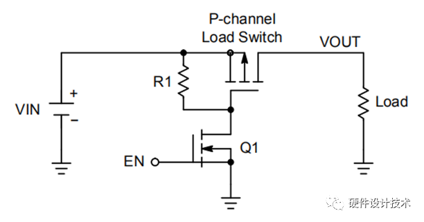
P-MOSOCP原理简介
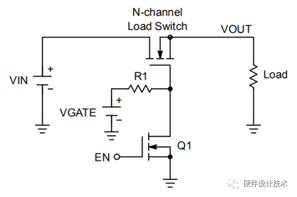
N-MOSOCP原理简介
| NMOS | PMOS | |
| Ron | 较小 | 较大 |
| Io | 较大 | 较小 |
| Charge pump | 需要 | 不需要 |
| Parasitic capacitance | 较小 | 较大 |
| Cost | 较高 | 较低 |
性能指标对比
三、镜像电流采样技术:
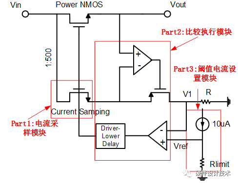
1、外部设置Rlimit,确定触发Rlimit时的电流为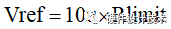
2、随着负载电流的增加,成比例的镜像电流也逐渐增加
3、当镜像电流达到满足, 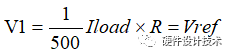 此时,触发限流机制
4、低延时的驱动单元将功率管的栅极电压拉低,达到限制PowerNMOS电流的大小的目的
四、PCB Layout注意事项
1、输入输出电容靠近芯片PIN脚摆放
2、输入输出电容两端端就近打足够的GND-VIA
3、芯片及周边元件尽量靠近负载端摆放,减小路径上的寄生参数
4、TVS靠近芯片PIN脚摆放,电流流过顺序为先TVS,再过电容,最后到芯片PIN脚
5、Rlimit电阻选用的精度至少±1%
五、OVP 与 OCP 对比:
This is quite different than the almost immediate response time of an OVP system. Even if the OCP delay time was set to zero, the response is still on the order of milliseconds instead of microseconds compared to an OVP event. And when the amount of overdrive is small, as is the case for the 6 A loading, providing just 1 A of overdrive, the total response time is much greater.
Unlike the OVP system, which operates totally independent of the voltage limit control system, the OCP system is triggered off the current limit control system. Thus the total response time includes the response time of the current limit as well. The behavior of a current limit is quite different than a simple “go/no go” threshold detector like OVP. A limit system, or circuit, needs to regulate the power supply’s output at a certain level, making it a feedback control system. The stability of this system is important, both with crossing over from constant voltage operation as well as maintaining a stable output current after crossing over. This leads to the slower and overdrive dependent response characteristics that are typical of current limit systems.
审核编辑:刘清
-
芯片
+关注
关注
463文章
54686浏览量
471255 -
pcb
+关注
关注
4425文章
24037浏览量
427490 -
负载电流
+关注
关注
1文章
629浏览量
15330 -
TVS
+关注
关注
8文章
1011浏览量
63935 -
MOS
+关注
关注
32文章
1804浏览量
101516
原文标题:Over Current Protection【OCP】
文章出处:【微信号:硬件设计技术,微信公众号:硬件设计技术】欢迎添加关注!文章转载请注明出处。
发布评论请先 登录
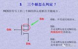
选择N-MOS还是P-MOS?
如何通过一个微分电路和一个P-MOS做到如下要求
请MOS管大神指点:MOS管H 半桥电磁阀驱动电路
给大家分享一个N-MOS和P-MOS驱动的应用实例
如何区分P-MOS和N-MOS?如何区分MOS的G、D、S管脚?MOS管如何导通?
模块工艺——双阱工艺(Twin-well or Dual-Well)
STM32的GPIO工作原理 开漏输出和推挽输出区别
电气符号傻傻分不清?一个N-MOS管和P-MOS管驱动应用实例
MOS管在电源控制中的应用:正负极驱动原理与设计要点


评论