 MPSoC R5引导4个A53和两个R5的应用程序的例子

01 介绍
有工程师反馈R5引导A53和R5的应用程序后,A53和R5的应用程序没有正确执行。因此做了一个MPSoC R5引导4个A53和两个R5的应用程序的例子。
02 FSBL
MPSoC的FSBL能引导多个CPU的应用程序。工程师可以不理解上述寄存器的细节。如果boot.bin里的某个parttiion是某一个CPU的可执行代码,FSBL中的函数XFsbl_Handoff( )会启动对应的CPU。如果是目标CPU是A53,会使用函数
XFsbl_UpdateResetVector()更新A53的服务地址。
03 应用程序例子
由于只是简单例子,所以所有CPU都使用同一个串口。为了防止所有CPU打印出来的信息,混杂在一起,所以在打印之后,增加了1秒钟延时。
打印中,增加了CPU的信息,用于区分不同CPU。
int main()
{
    init_platform();

sleep(1);

    for( int i=0; ; i++ )
    {
    xil_printf("No.%d Hello World from r5-aaa.

", i );
    sleep(1);
    }

    cleanup_platform();
    return 0;
}
04 内存分配
4个A53和两个R5的应用程序,都运行在DDR里。每个应用程序,必须使用不同的DDR空间。
CPU DDR起始地址 DDR大小
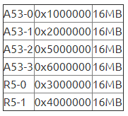
请根据上表,更新lscript.ld中的MEMORY里的ddr字段。A53-0的lscript.ld中的MEMORY部分,设置如下:
MEMORY
{
   psu_ddr_0_MEM_0 : ORIGIN = 0x1000000, LENGTH = 0x1000000
}
R5-0的lscript.ld中的MEMORY部分,设置如下:
MEMORY
{
   psu_ocm_ram_0_MEM_0 : ORIGIN = 0xFFFC0000, LENGTH = 0x40000
   psu_r5_0_atcm_MEM_0 : ORIGIN = 0x0, LENGTH = 0x10000
   psu_r5_0_btcm_MEM_0 : ORIGIN = 0x20000, LENGTH = 0x10000
   psu_r5_ddr_0_MEM_0 : ORIGIN = 0x3000000, LENGTH = 0x1000000
   psu_r5_tcm_ram_0_MEM_0 : ORIGIN = 0x0, LENGTH = 0x40000
}
05 R5引导4个A53和两个R5的bif文件例子
在SDK里,制作启动文件boot.bin时,需要正确设置每个ELF文件的目标CPU。SDK不能根据ELF文件,自动设置目标CPU。如果设置错误,可能引起错误,导致相关CPU的代码,不能正确执行。
//arch = zynqmp; split = false; format = BIN
the_ROM_image:
{
[fsbl_config]r5_single
[bootloader]C:prjzcu106v183zcu106_bsp_hw_hdf
5a_fsblDebugd_r5a_fsbl.elf
[destination_cpu = a53-0]C:prjzcu106v183zcu106_bsp_hw_hdfa53a_helloDebugd_a53a_hello.elf
[destination_cpu = a53-1]C:prjzcu106v183zcu106_bsp_hw_hdfa53b_helloDebugd_a53b_hello.elf
[destination_cpu = a53-2]C:prjzcu106v183zcu106_bsp_hw_hdfa53c_helloDebugd_a53c_hello.elf
[destination_cpu = a53-3]C:prjzcu106v183zcu106_bsp_hw_hdfa53d_helloDebugd_a53d_hello.elf
[destination_cpu = r5-0]C:prjzcu106v183zcu106_bsp_hw_hdf
5a_helloDebugd_r5a_hello.elf
[destination_cpu = r5-1]C:prjzcu106v183zcu106_bsp_hw_hdf
5b_helloDebugd_r5b_hello.elf
}
06 R5引导4个A53和两个R5的启动记录
Xilinx Zynq MP First Stage Boot Loader
Release 2018.3   Oct 12 2020  -  1708
Reset Mode      :       System Reset
Platform: Silicon (4.0), Cluster ID 0xC0000100
Running on R5-0 Processor, Device Name: XCZU7EV
Initializing TCM ECC
Address 0xFFFD95F0, Length FFE00020, ECC initialized
Address 0xFFFD95F0, Length FFE20000, ECC initialized
FMC VADJ Configuration Successful
Board Configuration successful
Processor Initialization Done
================= In Stage 2 ============
SD1 with level shifter Boot Mode
SD: rc= 0
File name is BOOT.BIN
Multiboot Reg : 0x0
Image Header Table Offset 0x8C0
*****Image Header Table Details********
Boot Gen Ver: 0x1020000
No of Partitions: 0x9
Partition Header Address: 0x440
Partition Present Device: 0x0
Initialization Success
======= In Stage 3, Partition No:1 =======
UnEncrypted data Length: 0x2812
Data word offset: 0x2812
Total Data word length: 0x2812
Destination Load Address: 0x1000000
Execution Address: 0x1000000
Data word offset: 0x5CF0
Partition Attributes: 0x116
Partition 1 Load Success
======= In Stage 3, Partition No:2 =======
UnEncrypted data Length: 0x2812
Data word offset: 0x2812
Total Data word length: 0x2812
Destination Load Address: 0x2000000
Execution Address: 0x2000000
Data word offset: 0x8510
Partition Attributes: 0x216
Partition 2 Load Success
======= In Stage 3, Partition No:3 =======
UnEncrypted data Length: 0x2812
Data word offset: 0x2812
Total Data word length: 0x2812
Destination Load Address: 0x5000000
Execution Address: 0x5000000
Data word offset: 0xAD30
Partition Attributes: 0x316
Partition 3 Load Success
======= In Stage 3, Partition No:4 =======
UnEncrypted data Length: 0x2812
Data word offset: 0x2812
Total Data word length: 0x2812
Destination Load Address: 0x6000000
Execution Address: 0x6000000
Data word offset: 0xD550
Partition Attributes: 0x416
Partition 4 Load Success
======= In Stage 3, Partition No:5 =======
UnEncrypted data Length: 0x148
Data word offset: 0x148
Total Data word length: 0x148
Destination Load Address: 0x0
Execution Address: 0x3C
Data word offset: 0xFD70
Partition Attributes: 0x51E
XFsbl_PartitionCopy:Going for LOVEC HIGHVEC Mechanism for R5.
XFsbl_PartitionLoad:After Partition Validation
Going for LOVEC HIGHVEC Mechanism for R5.
Partition 5 Load Success
======= In Stage 3, Partition No:6 =======
UnEncrypted data Length: 0x9B1
Data word offset: 0x9B1
Total Data word length: 0x9B1
Destination Load Address: 0x3000000
Execution Address: 0x0
Data word offset: 0xFEC0
Partition Attributes: 0x51E
Partition 6 Load Success
======= In Stage 3, Partition No:7 =======
UnEncrypted data Length: 0x148
Data word offset: 0x148
Total Data word length: 0x148
Destination Load Address: 0x0
Execution Address: 0x3C
Data word offset: 0x10880
Partition Attributes: 0x61E
Initializing TCM ECC
Address 0xFFFD95F0, Length FFE90000, ECC initialized
Address 0xFFFD95F0, Length FFEB0000, ECC initialized
Partition 7 Load Success
======= In Stage 3, Partition No:8 =======
UnEncrypted data Length: 0x9B1
Data word offset: 0x9B1
Total Data word length: 0x9B1
Destination Load Address: 0x4000000
Execution Address: 0x0
Data word offset: 0x109D0
Partition Attributes: 0x61E
Partition 8 Load Success
All Partitions Loaded
================= In Stage 4 ============
PMU-FW is not running, certain applications may not be supported.
Protection configuration applied
CPU 0x100 reset release, Exec State 0x0, HandoffAddress: 1000000
CPU 0x200 reset release, Exec State 0x0, HandoffAddress: 2000000
CPU 0x300 reset release, Exec State 0x0, HandoffAddress: 5000000
CPU 0x400 reset release, Exec State 0x0, HandoffAddress: 6000000
CPU 0x600 reset release, Exec State 0x8, HandoffAddress: 3C
XFsbl_Handoff:Restored R5LovecBuffer to LOVEC for R5.
Running Cpu Handoff address: 0x3C, Exec State: 8
Exit from FSBL
No.0 Hello World from a53-aaa.
No.0 Hello World from a53-bbb.
No.0 Hello World from a53-ccc.
No.0 Hello World from a53-ddd.
No.0 Hello World from r5-bbb.
No.0 Hello World from r5-aaa.
No.1 Hello World from a53-aaa.
No.1 Hello World from a53-bbb.
No.1 Hello World from a53-ccc.
No.1 Hello World from a53-ddd.
No.1 Hello World from r5-bbb.
No.1 Hello World from r5-aaa.
No.2 Hello World from a53-aaa.
No.2 Hello World from a53-bbb.
No.2 Hello World from a53-ccc.
No.2 Hello World from a53-ddd.
No.2 Hello World from r5-bbb.
07 APU Module
由于MPSoC的FSBL能引导多个CPU的应用程序,工程师可以不理解下述寄存器的细节。
APU Module的基地址是0xFD5C0000,下列寄存器用于设置APU的复位地址。
RVBARADDR0L0x00000040Reset Vector Base Address
RVBARADDR0H0x00000044Reset Vector Base Address
RVBARADDR1L0x00000048Reset Vector Base Address
RVBARADDR1H0x0000004CReset Vector Base Address
RVBARADDR2L0x00000050Reset Vector Base Address
RVBARADDR2H0x00000054Reset Vector Base Address
RVBARADDR3L0x00000058Reset Vector Base Address
RVBARADDR3H0x0000005CReset Vector Base Address
08 RPU Module
RPU Module的基地址是0xFF9A0000,下列寄存器用于设置RPU的复位地址。
RPU0_CFG    0x00000100Configuration Parameters specific to RPU0
RPU1_CFG0x00000200Configuration Parameters specific to RPU1
审核编辑 :李倩
-
寄存器
+关注
关注
31文章
5619浏览量
130414 -
cpu
+关注
关注
68文章
11327浏览量
225882 -
应用程序
+关注
关注
38文章
3346浏览量
60419
原文标题:【工程师分享】MPSoC R5引导4个A53和两个R5的应用程序的例子
文章出处:【微信号:zhuyandz,微信公众号:FPGA之家】欢迎添加关注!文章转载请注明出处。
发布评论请先 登录
S32K系列引导加载程序应用程序跨不同定制电路板设计的跳转问题求解
关于S32G3引导加载程序构建问题求解
如何在 i.MX RT1050 上实现两个镜像(引导加载程序应用程序)的双 HAB 身份验证?
如何在 S32G3 上的 M7 和 A53 内核之间建立 IPCF 通信?
AD817配合ADG1211设计一个电流源
圣邦微电子SGM51613R4A/SGM51613R8A:高性能16位ADC的深度剖析

DK5V60R10VT1东科高性能同步整流芯片
V5.2.1 A53 SMP启动卡死的原因?怎么解决?
基于AM64x Sitara™处理器的工业应用解决方案
如何用Arduino Nano/UNO R3开发板给另一个Arduino IDE不能下载的Arduino Nano/UNO R3开发板重新烧录引导程序bootlaoder
一般晶体管光耦的开关特性
Banana Pi BPI-R4 Pro Wifi7 路由器开发板采用联发科MT7988A芯片设计,支持4个2.5G网口,支持2个10G光电口,支持4G/5G扩展
基于RFSOC的8路5G ADC和8路9G的DAC PCIe卡


评论