 ADI ADP1031三路隔离微功耗管理解决方案

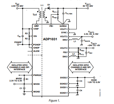
ADI公司的ADP1031是具有七个数字隔离器的三路隔离微功耗管理(PMU)单元,包括隔离的反激DC/DC稳压器,反相的DC/DC稳压器和降压DC/DC稳压器。此外,还包括四个高速SPI隔离通路和三个通用的隔离器。输入电压从4.5V到60V,产生隔离VOUT1输出电压6V-28V(可调整版)或21V-24V(固定版),VOUT2为工厂可编程电压+5.15V,+5.0V或+3.3V,VOUT3为可调整输出电压-24V到-5V,主要用在工业自动化和过程控制,仪器和数据采集系统以及其数据和电源隔离。本文介绍了ADP1031主要特性, 简化框图, 应用电路图以及评估板ADP1031CP-EVALZ主要特性,电路图,材料清单和PCB设计图。
Three-Channel, Isolated Micropower Management Unit with Seven Digital IsolatorsThe ADP1031 is a high performance, isolated micropower management unit (PMU) that combines an isolated flyback dc-to-dc regulator, an inverting dc-to-dc regulator, and a buck dc-to-dc regulator, providing three isolated power rails. Additionally, the ADP1031 contains four, high speed, serial peripheral interface (SPI) isolation channels and three general- purpose isolators for channel to channel applications where low power dissipation and small solution size is required.
Operating over an input voltage range of +4.5 V to +60 V, the ADP1031 generates isolated output voltages of +6 V to +28 V (adjustable version) or+ 21 V and +24 V (fixed versions) for VOUT1, factory programmable voltages of +5.15 V, +5.0 V, or +3.3 V for VOUT2, and an adjustable output voltages of −24 V to −5 V for VOUT3. By default, the ADP1031 flyback regulator operates at a 250 kHz switching frequency and the buck and inverting regulators operate at 125 kHz. All three regulators are phase shifted relative to each other to reduce electromagnetic interference (EMI)。 The ADP1031 can be driven by an external oscillator in the range of 350 kHz to 750 kHz to ease noise filtering in sensitive applications. The digital isolators integrated in the ADP1031 use Analog Devices,Inc., iCoupler® chip scale transformer technology, optimized for low power and low radiated emissions. The ADP1031 is available in a 9 mm×7 mm, 41-lead LFCSP and is rated for a −40℃ to +125℃ operating junction temperature range.
ADP1031主要特性:
Wide input supply voltage range: 4.5 V to 60 V
Integrated flyback power switch
Generates isolated, independent bipolar outputs and factory programmable buck output
VOUT1: 21 V, 24 V or 6 V to 28 V
VOUT2: 5.15 V, 5.0 V, or 3.3 V
VOUT3: −24 V to −5 V
Uses a 1:1 ratio transformer for simplified transformer design
Peak current limiting and OVP for flyback, buck, and inverting regulators
Precision enable input and power-good output
Adjustable switching frequency via SYNC input Internal compensation and soft start control per regulator High speed, low propagation delay, SPI signal isolation channels
Three, 100 kbps general-purpose isolated data channels 9 mm × 7 mm LFCSP form factor enables small overall solution size
−40℃ to +125℃ operating junction temperature range
Conforms to CISPR11 Class B radiated emission limits
Safety and regulatory approvals (pending)
UL recognition: 2500 V rms for 1 minute per UL 1577
CSA Component Acceptance Notice 5A
300 V rms basic insulation between slave, master, and field power domains (IEC 61010-1, pending)
VDE certificate of conformity
DIN V VDE 0884-10 (VDE 0884-10):2006-12
VIORM = 565 VPEAK
ADP1031应用:
Industrial automation and process control
Instrumentation and data acquisition systems
Data and power isolation
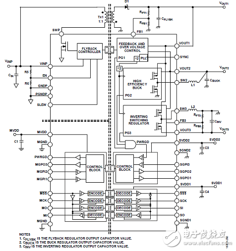
图1.ADP1031简化框图
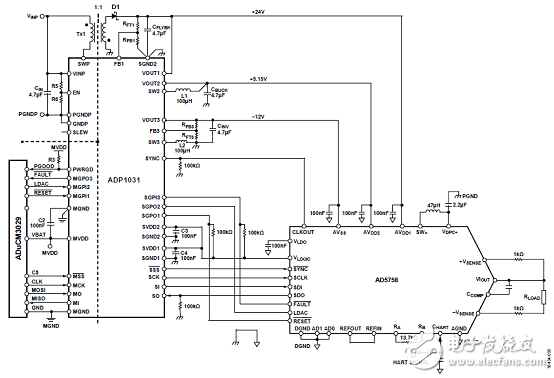
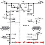
图2.采用AD5758的ADP1031应用电路图
评估板ADP1031CP-EVALZ
The ADP1031CP-EVALZ is a fully featured evaluation board that demonstrates the functionality of the ADP1031 dc-to-dc converters and the isolated data channels.
Users can evaluate ADP1031 device measurements, such as line regulation, load regulation, and efficiency with the evaluation board. The board also assists in evaluating the functionality of the isolated digital channels. Device features including oscillator synchronization, soft start, power good monitoring, sequencing, and slew rate control can be demonstrated on the evaluation board.
Each board model in the evaluation kit has a different output configuration. Only one board model is included in the kit but users can order from five different board models to fit their application needs.
Refer to the ADP1031 data sheet for more details about the dc-to-dc converters and isolated data channels.
评估板ADP1031CP-EVALZ主要特性:
Input voltage range: 4.5 V to 60 V
Output voltage VOUT1: 24 V or 21 V
Output voltage VOUT2: 5.15 V
Output voltage VOUT3: −15 V
Enable and disable controls
Slew rate controls
Access to SYNC pin for oscillator synchronization
Access to all seven data channels
图3.评估板ADP1031CP-EVALZ外形图
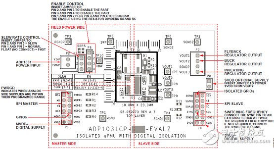
图4.评估板ADP1031CP-EVALZ概略图
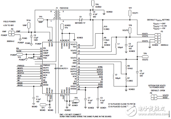
图5.评估板ADP1031CP-EVALZ电路图(1)
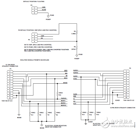
图6.评估板ADP1031CP-EVALZ电路图(2):连接器和外设
评估板ADP1031CP-EVALZ材料清单:
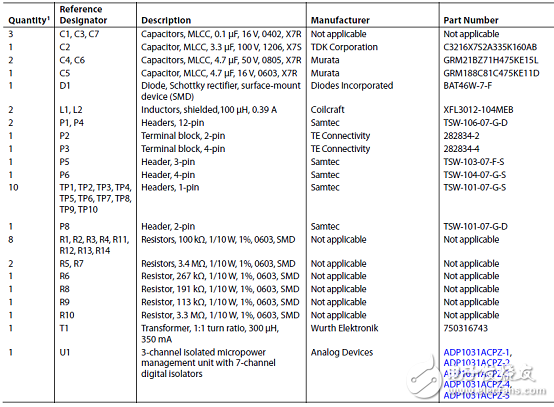
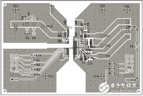
图7.评估板ADP1031CP-EVALZ PCB设计图(1):顶层
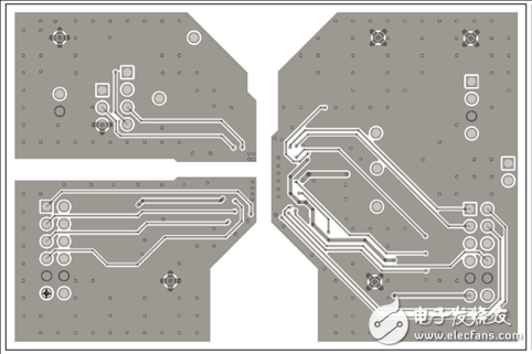
图8.评估板ADP1031CP-EVALZ PCB设计图(2):底层
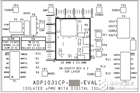
图9.评估板ADP1031CP-EVALZ PCB设计图(3):顶层丝印
详情请见:
https://www.analog.com/media/en/technical-documentation/data-sheets/ADP1031.pdf
和https://www.analog.com/media/en/technical-documentation/user-guides/ADP1031CP-EVALZ-UG-1226.pdf
ADP1031.pdf
ADP1031CP-EVALZ-UG-1226.pdf
-
ADI
+关注
关注
151文章
46126浏览量
281268 -
PMU
+关注
关注
1文章
127浏览量
23432
发布评论请先 登录
能够设计出适合过程控制的高精度、高密度和隔离模拟输出模块的系统级方法
ADI可穿戴设备电源管理解决方案
用于多路抽头输出隔离电源的简易解决方案
【限时下载】ADI 用于多路抽头输出隔离电源的简易解决方案
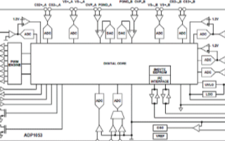
三路数字电源控制器ADP1053的性能特点及应用

ADP1031CP-EVALZ ADP1031CP-EVALZ评估板
ADP1031具有七个数字隔离器的三通道隔离式微功耗管理单元技术手册


评论