完善资料让更多小伙伴认识你,还能领取20积分哦,立即完善>

The ADGS1612 contains four independent single-pole/single-throw (SPST) switches. A serial peripheral interface (SPI) controls the switches. The SPI interface has robust error detection features, including cyclic redundancy check (CRC) error detection, invalid read/write address detection, and serial clock (SCLK)count error detection.
It is possible to daisy-chain multiple ADGS1612 devices together. Daisy-chaining enables the configuration of multiple devices with a minimal amount of digital lines. The ADGS1612 can also operate in burst mode to decrease the time between SPI commands.
Each switch conducts equally well in both directions when on, and each switch has an input signal range that extends to the supplies. In the off condition, signal levels up to the supplies are blocked.
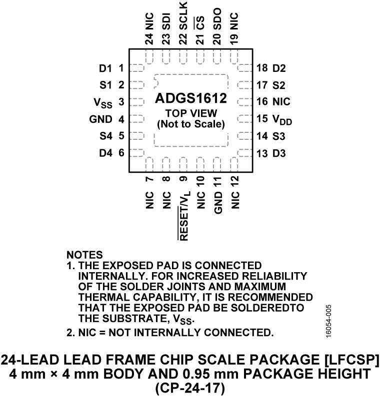
The ultralow on resistance (RON) of these switches make them ideal solutions for data acquisition and gain switchingapplications where low RON and low distortion are critical. The RON profile is very flat over the full analog input range, ensuring excellent linearity and low distortion when switching audio signals. The ADGS1612 exhibits break-before-make switchingaction for use in multiplexer applications. Note that throughout this data sheet, the multifunction pin, RESET/VL, is referred to either by the entire pin name or by a single function of the pin,for example, VL, when only that function is relevant.
Product Highlight
Applications

关注我们的微信

下载发烧友APP

电子发烧友观察

版权所有 © 湖南华秋数字科技有限公司
电子发烧友 (电路图) 湘公网安备43011202000918 电信与信息服务业务经营许可证:合字B2-20210191 工商网监
湘ICP备 2023018690 号
工商网监
湘ICP备 2023018690 号

