完善资料让更多小伙伴认识你,还能领取20积分哦,立即完善>
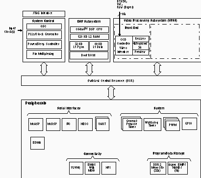
The TMS320C64x+ DSPs (including the TMS320DM6435 device) are the highest-performance fixed-point DSP generation in the TMS320C6000 DSP platform. The DM6435 device is based on the third-generation high-performance, advanced VelociTI very-long-instruction-word (VLIW) architecture developed by Texas Instruments (TI), making these DSPs an excellent choice for digital media applications. The C64x+ devices are upward code-compatible from previous devices that are part of the C6000 DSP platform. The C64x DSPs support added functionality and have an expanded instruction set from previous devices.
Any reference to the C64x DSP or C64x CPU also applies, unless otherwise noted, to the C64x+ DSP and C64x+ CPU, respectively.
With performance of up to 4800 million instructions per second (MIPS) at a clock rate of 600 MHz, the C64x+ core offers solutions to high-performance DSP programming challenges. The DSP core possesses the operational flexibility of high-speed controllers and the numerical capability of array processors. The C64x+ DSP core processor has 64 general-purpose registers of 32-bit word length and eight highly independent functional unitstwo multipliers for a 32-bit result and six arithmetic logic units (ALUs). The eight functional units include instructions to accelerate the performance in video and imaging applications. The DSP core can produce four 16-bit multiply-accumulates (MACs) per cycle for a total of 2400 million MACs per second (MMACS), or eight 8-bit MACs per cycle for a total of 4800 MMACS. For more details on the C64x+ DSP, see the TMS320C64x/C64x+ DSP CPU and Instruction Set Reference Guide (literature number SPRU732).
The DM6435 also has application-specific hardware logic, on-chip memory, and additional on-chip peripherals similar to the other C6000 DSP platform devices. The DM6435 core uses a two-level cache-based architecture. The Level 1 program memory/cache (L1P) consists of a 256K-bit memory space that can be configured as mapped memory or direct mapped cache, and the Level 1 data (L1D) consists of a 640K-bit memory space384K-bit of which is mapped memory and 256K-bit of which can be configured as mapped memory or 2-way set-associative cache. The Level 2 memory/cache (L2) consists of a 1M-bit memory space that is shared between program and data space. L2 memory can be configured as mapped memory, cache, or combinations of the two.
The peripheral set includes: a configurable video port (VPFE); a 10/100 Mb/s Ethernet MAC (EMAC) with a management data input/output (MDIO) module; a 4-bit transmit, 4-bit receive VLYNQ interface; an inter-integrated circuit (I2C) Bus interface; a multichannel buffered serial port (McBSP); a multichannel audio serial port (McASP0) with 4 serializers; 2 64-bit general-purpose timers each configurable as 2 independent 32-bit timers; 1 64-bit watchdog timer; a user-configurable 16-bit host-port interface (HPI); up to 111-pins of general-purpose input/output (GPIO) with programmable interrupt/event generation modes, multiplexed with other peripherals; 2 UARTs with hardware handshaking support on 1 UART; 3 pulse width modulator (PWM) peripherals; 1 high-end controller area network (CAN) controller [HECC]; and 2 glueless external memory interfaces: an asynchronous external memory interface (EMIFA) for slower memories/peripherals, and a higher speed synchronous memory interface for DDR2.
The DM6435 device includes a Video Processing Subsystem (VPSS) with a configurable video/imaging front-end input peripheral used for video capture.
The Video Processing Front-End (VPFE) is comprised of a CCD Controller (CCDC), a Preview Engine (Previewer), Histogram Module, Auto-Exposure/White Balance/Focus Module (H3A), and Resizer. The CCDC is capable of interfacing to common video decoders, CMOS sensors, and Charge Coupled Devices (CCDs). The Previewer is a real-time image processing engine that takes raw imager data from a CMOS sensor or CCD and converts from an RGB Bayer Pattern to YUV422. The Histogram and H3A modules provide statistical information on the raw color data for use by the DM6435. The Resizer accepts image data for separate horizontal and vertical resizing from 1/4x to 4x in increments of 256/N, where N is between 64 and 1024.
The Ethernet Media Access Controller (EMAC) provides an efficient interface between the DM6435 and the network. The DM6435 EMAC support both 10Base-T and 100Base-TX, or 10 Mbits/second (Mbps) and 100 Mbps in either half- or full-duplex mode, with hardware flow control and quality of service (QOS) support.
The Management Data Input/Output (MDIO) module continuously polls all 32 MDIO addresses in order to enumerate all PHY devices in the system.
The I2C and VLYNQ ports allow DM6435 to easily control peripheral devices and/or communicate with host processors.
The high-end controller area network (CAN) controller [HECC] module provides a network protocol in a harsh environment to communicate serially with other controllers, typically in automotive applications.
The rich peripheral set provides the ability to control external peripheral devices and communicate with external processors. For details on each of the peripherals, see the related sections later in this document and the associated peripheral reference guides.
The DM6435 has a complete set of development tools. These include C compilers, a DSP assembly optimizer to simplify programming and scheduling, and a Windows debugger interface for visibility into source code execution.
All trademarks are the property of their respective owners.
| Applications |
| Operating Systems |
| Arm CPU |
| Arm MHz (Max.) |
| DSP |
| DSP MHz |
| Video Acceleration |
| Video Resolution/Frame Rate |
| Video Port (Configurable) |
| USB |
| PCI/PCIe |
| EMAC |
| DRAM |
| SPI |
| I2C |
| UART (SCI) |
| On-Chip L2 Cache/RAM |
| Operating Temperature Range (C) |
| Pin/Package |
| TMS320DM6435 |
|---|
| Automotive Communications and Telecom Consumer Electronics Energy Industrial Security Video and Imaging |
| DSP/BIOS VLX |
| 0 |
| 0 |
| 1 C64x |
| 400 500 600 700 |
| 0 |
| D1 or Less |
| 1 Dedicated Input |
| 0 |
| 0 |
| 10/100 |
| DDR2 |
| 0 |
| 1 |
| 2 |
| 128 KB (DSP) |
| 0 to 90 |
| 361NFBGA |

关注我们的微信

下载发烧友APP

机器人发烧友