 英飞凌电源管理芯片TLF35584的使用介绍

TLF35584介绍
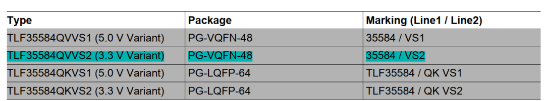
TLF35584是英飞凌推出的针对车辆安全应用的电源管理芯片,符合ASIL D安全等级要求,具有高效多电源输出通道,宽电压输入范围,根据不同的型号有3.3V和5.0V两种命名。可以为MCU提供600mA的电源,可以提供200mA的电源给通信,还可以提供精确的参考电压给ADC使用,具有SPI通信,可以监控和配置该芯片。我们以TLF35584QVVS2型号的使用来做介绍。TLF35584的封装类型以及电压分类如下表所示:
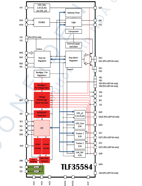
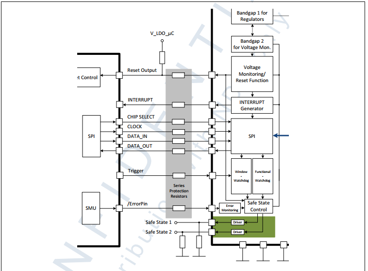
TLF35584系统框图
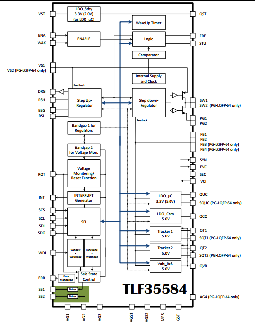
管脚介绍
| Pin | Symbol | Function |
| 1 | BSG |
Boost driver ground: Connect this pin to ground at the low side of an external current sense resistor to decouple the driver noise from the sensitive ground. If step up pre regulator option is not used, connect to ground. |
| 2 | VST |
Supply voltage standby regulator, input: Connect this input to supply (battery) voltage with reverse protection diode and capacitor between pin and ground. An EMC filter is recommended. |
| 3 | ENA |
Enable Input: A positive edge signal at this pin will wake the device. In case of not used connect to ground. |
| 4 | WAK |
Wake/Inhibit Input: A high level signal of defined length at this pin will wake the device. In case of not used, connect to ground |
| 5 | QST |
Output standby LDO: Connect a capacitor as close as possible to pin. |
| 6 | AG1 |
Analogue ground, pin 1: Connect this pin directly (low ohmic and low inductive) to ground. |
| 7 | AG2 |
Analogue ground, pin 2: Connect this pin directly (low ohmic and low inductive) to ground. |
| 8 | AGS1 |
Analogue ground, safety, pin 1: Connect this pin directly (low ohmic and low inductive) to ground. In case a safety switch is used, connect directly to the source of the NMOS used. |
| 9 | AGS2 |
Analogue ground, safety, pin 2: Connect this pin directly (low ohmic and low inductive) to ground. In case a safety switch is used, connect directly to the source of the NMOS used. |
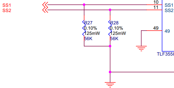
| 10 | SS2 |
Safe state signal 2: Safe state output signal 2, sets the application into a safe state. Signal is delayed against SS1, delay can be adjusted via SPI command. |
| 11 | SS1 |
Safe state signal 1: Safe state output signal 1, sets the application into a safe state. |
| 12 | SDI |
Serial peripheral interface, signal data input: SPI signalling port, connect to SPI port “data output” of micro processor to receive commands during SPI communication. |
| 13 | SDO |
Serial peripheral interface, signal data output: SPI signalling port, connect to SPI port “data input” of micro processor to send status information during SPI communication. |
| 14 | SCL |
Serial peripheral interface, signal clock: SPI signalling port, connect to SPI port “clock” of micro processor to clock the device for SPI communication. |
| 15 | SCS |
Serial peripheral interface, signal chip select: SPI signalling port, connect to SPI port “chip select” of micro processor to address the device for SPI communication. |
| 16 | WDI |
Watchdog input, trigger signal: Input for trigger signal, connect the “trigger signal output” of the micro processor to this pin. In case of not used, leave open (internal pull-down). |
| 17 | ROT |
Reset output: Open drain structure with internal pull-up current source. A low signal at this pin indicates a reset event. |
| 18 | INT |
Interrupt signal: Push-pull-stage. A low pulse at this pin indicates an interrupt, the micro processor shall read out the SPI status registers. Connect to a non maskable interrupt port (NMI) of the micro processor core supply voltage. |
| 19 | SYN |
Synchronization output signal: Connect this output to the optional external switch mode post regulator synchronization input. The signal delivers the step down regulator switching frequency either in phase or shifted by 180° (selectable via SPI command). The switch mode post regulator shall synchronize to the rising edge. If not used, leave open. |
| 20 | ERR |
Error signal input: Input for error signal from micro processor safety managing unit (SMU, internal failure detection of the micro processor). Connect the “error signal output” of the micro processor to this pin. |
| 21 | EVC |
Enable external post regulator for core supply: Connect this pin to the enable input of the external post regulator. If not used, leave open. |
| 22 | MPS |
Microcontroller programming support pin: Pull down this pin to ground for operation. Optionally, this pin can be used for microcontroller debugging and programming purposes. For details please refer to Chapter 11.7. |
| 23 | SEC |
Configuration pin for external post regulator for core supply: Connect this pin to ground if the option external post regulator is not used. If the option external post regulator is used, leave open. |
| 24 | FRE |
Frequency adjustment pin: Connect pin to ground for low frequency range or leave open for high frequency range. |
| 25 | STU |
Configuration pin for step up converter: Connect this pin to ground if the option step up pre regulator is not used. If the option step up pre regulator is used, leave open. |
| 26 | VCI |
Input for optional external post regulator output voltage (core supply): Connect an external resistor divider to adjust the over and under voltage thresholds of reset output signal ROT. If the option external post regulator is not used, leave open. |
| 27 | GST |
Gate stress pin: Not for customer use. Connect this pin directly (low ohmic and low inductive) to ground. |
| 28 | AG3 |
Analogue ground, pin 3: Connect this pin directly (low ohmic and low inductive) to ground. |
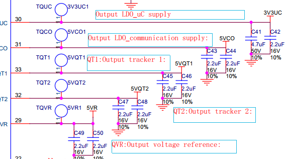
| 29 | QVR |
Output voltage reference: Connect a capacitor as close as possible to pin. |
| 30 | QUC |
Output LDO_uC supply (micro processor supply): Connect a capacitor as close as possible to pin. |
| 31 | QCO |
Output LDO_communication supply: Connect a capacitor as close as possible to pin. |
| 32 | QT2 |
Output tracker 2: Connect a capacitor as close as possible to pin. |
| 33 | QT1 |
Output tracker 1: Connect a capacitor as close as possible to pin. |
| 34 | N.C. |
Internally not connected: This pin is electrically not connected internally and can be kept open/floating, connected to GND or any other signal. Consider neighboring signals for potential failures. |
| 20 | ERR |
Error signal input: Input for error signal from micro processor safety managing unit (SMU, internal failure detection of the micro processor). Connect the “error signal output” of the micro processor to this pin. |
| 21 | EVC |
Enable external post regulator for core supply: Connect this pin to the enable input of the external post regulator. If not used, leave open. |
| 22 | MPS |
Microcontroller programming support pin: Pull down this pin to ground for operation. Optionally, this pin can be used for microcontroller debugging and programming purposes. For details please refer to Chapter 11.7. |
| 23 | SEC |
Configuration pin for external post regulator for core supply: Connect this pin to ground if the option external post regulator is not used. If the option external post regulator is used, leave open. |
| 24 | FRE |
Frequency adjustment pin: Connect pin to ground for low frequency range or leave open for high frequency range. |
| 25 | STU |
Configuration pin for step up converter: Connect this pin to ground if the option step up pre regulator is not used. If the option step up pre regulator is used, leave open. |
| 26 | VCI |
Input for optional external post regulator output voltage (core supply): Connect an external resistor divider to adjust the over and under voltage thresholds of reset output signal ROT. If the option external post regulator is not used, leave open. |
| 27 | GST |
Gate stress pin: Not for customer use. Connect this pin directly (low ohmic and low inductive) to ground. |
| 28 | AG3 |
Analogue ground, pin 3: Connect this pin directly (low ohmic and low inductive) to ground. |
| 29 | QVR |
Output voltage reference: Connect a capacitor as close as possible to pin. |
| 30 | QUC |
Output LDO_uC supply (micro processor supply): Connect a capacitor as close as possible to pin. |
| 31 | QCO |
Output LDO_communication supply: Connect a capacitor as close as possible to pin. |
| 32 | QT2 |
Output tracker 2: Connect a capacitor as close as possible to pin. |
| 33 | QT1 |
Output tracker 1: Connect a capacitor as close as possible to pin. |
| 34 | N.C. |
Internally not connected: This pin is electrically not connected internally and can be kept open/floating, connected to GND or any other signal. Consider neighboring signals for potential failures. |
| 46 | DRG |
Driver output for external step up regulator power stage, connect to gate: Gate of low side switch of step up pre regulator: Connect to the gate of an external N-channel mosfet, line to be straight and as short as possible. If step up pre regulator option is not used, leave open. |
| 47 | RSH |
Sense resistor for external step up regulator power stage, high side: Connect this pin to the high side of an external current sense resistor to determine the maximum current threshold through the external N-channel mosfet. If step up pre regulator option is not used, connect to ground. |
| 48 | RSL |
Sense resistor for external step up regulator power stage, low side: Connect this pin to the low side of an external current sense resistor to determine the maximum current threshold through the external N-channel mosfet. If step up pre regulator option is not used, connect to ground. |
| EP1 |
Edge pin no 1: Keep area below this pin free of ground or other signals, do not solder this pin to ground or any other signal. This pin must be kept free of soldering. |
|
| EP2 |
Edge pin no 2: Keep area below this pin free of ground or other signals, do not solder this pin to ground or any other signal. This pin must be kept free of soldering. |
|
| EP3 |
Edge pin no 3: Keep area below this pin free of ground or other signals, do not solder this pin to ground or any other signal. This pin must be kept free of soldering. |
|
| EP4 |
Edge pin no 4: Keep area below this pin free of ground or other signals, do not solder this pin to ground or any other signal. This pin must be kept free of soldering. |
|
|
Coolin g Tab |
GND |
Cooling Tab. Connect externally to GND and heat sink area. |
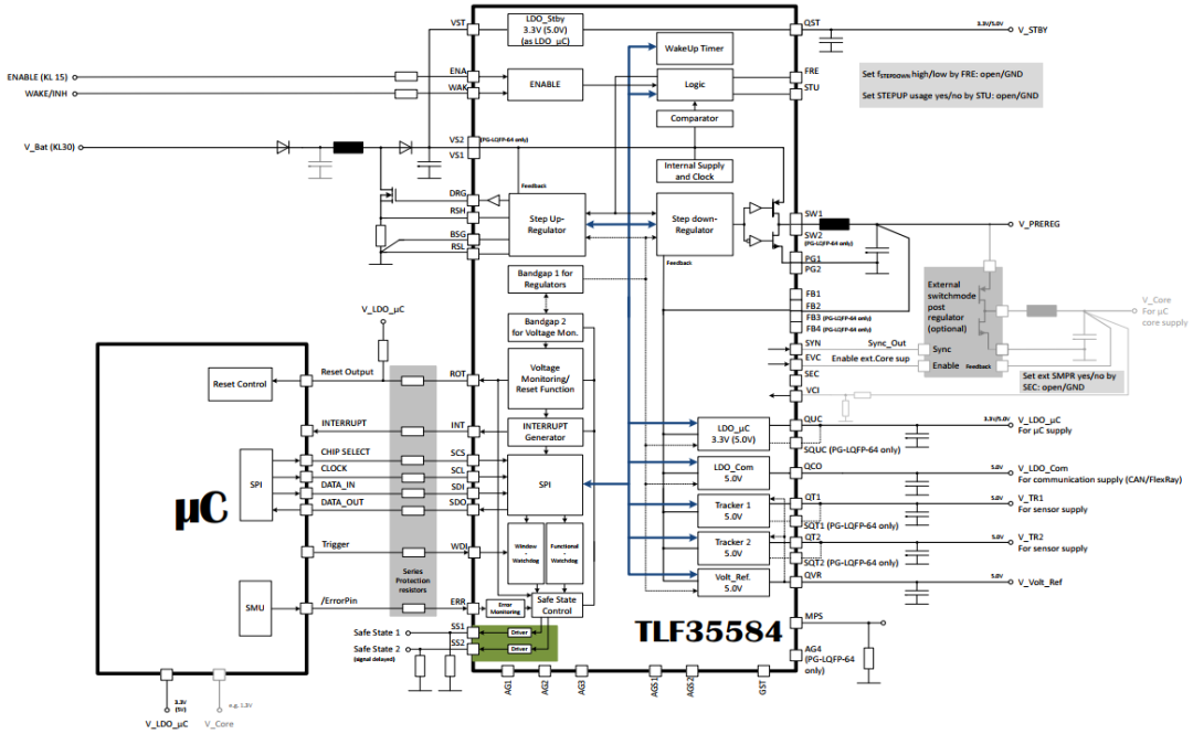
典型应用框图
安全功能
TLF35584提供了很多安全功能来保证系统的安全
输出电源轨监控
Vprereg
VQUC
VQST
VQVR
VVCI
VQT1, VQT2
VQCO
提供MCU外部安全机制的时序时间监控服务
监控MCU的SMU ERR输出功能
监控MCU的看门狗输出服务
二次安全关断能力
TSR
TSR01 -在所有产生和监控的输出电压上检测和响应故障。违反将会导致系统级的单点失效
TSR02 -检测并响应MCU安全管理单元(SMU)的错误触发。违反会导致潜伏失效或者多点失效
TSR03 -检测并响应由MCU错误触发的定时监控服务,违反会导致潜伏失效或者多点失效
TSR04 -内部需要时激活二次关断信号,违反TSR04可能会导致潜伏失效
安全功能应用
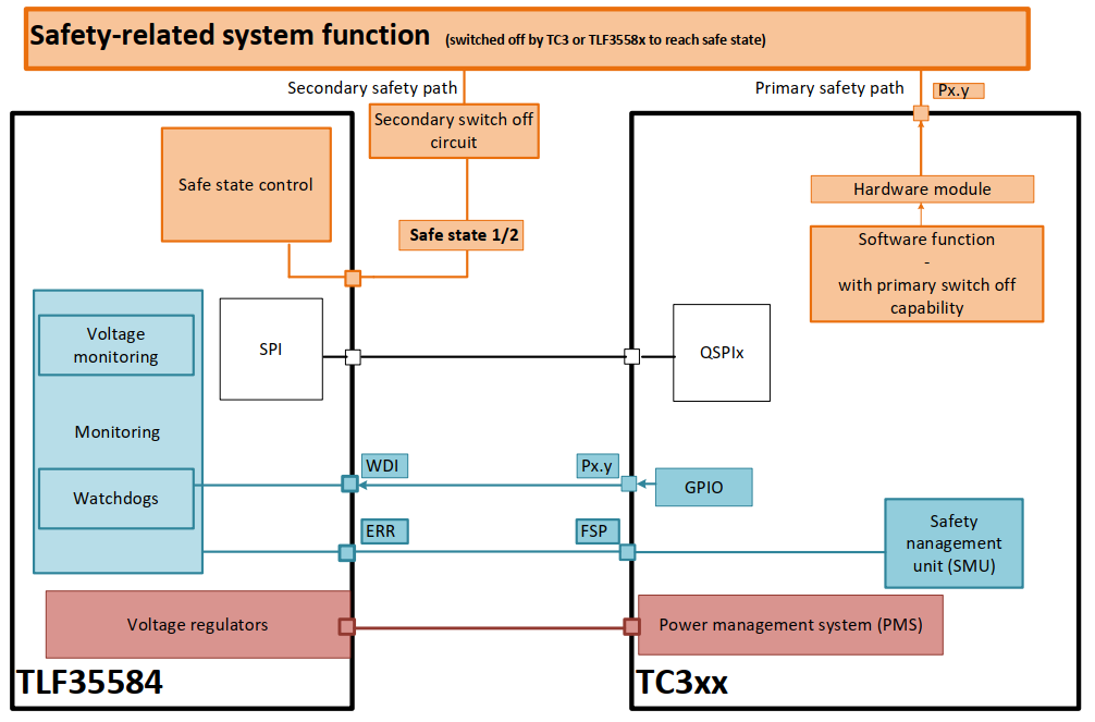
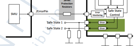
安全路径
安全路径是信号链和电路使能并维持系统的安全状态。对于一些TLF35584目标应用,达到了安全状态
通过禁用执行器、通信通道或整个系统。在这样的系统中,安全路径是安全停机路径。
首要安全路径
主要安全路径不是由PMIC管理的,而是由MCU单片机控制的。因此,主安全路径不依赖于PMIC的安全逻辑。通常,这类安全路径是通过安全MCU建立的。该单片机可以使应用程序始终处于安全状态,使用的条件在有效范围内,外部安全机制可用。
二次安全路径
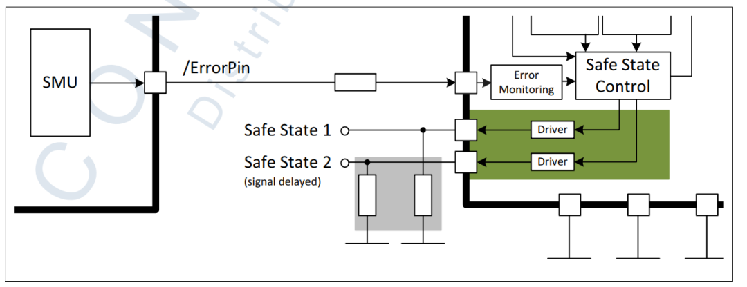
二次安全路径或者叫二次关断路径是通过PMIC的安全功能实现的。在PMIC的安全功能TSR需求中,系统的安全状态是通过PMIC的安全状态输出达到的,也就是说通过TLF35584的SS1和SS2输出连接到系统电路可以释放或者进入安全状态,这种机制可以在检测到关键失效时候进入安全状态已达到安全目标。
安全状态
系统的安全状态被认为是没有任何不合理的高水平风险的运行模式
Assumption: [SM_00_01]
只要TLF35584处于安全状态(通过激活二次安全关机路径,即SS1/SS2处于低电平表示),则子系统处于安全状态。
TLF35584包括许多安全设计功能和安全机制,以支持实现技术安全分析总结报告中定义的安全级别的安全要求.
安全特性
安全特性概览
安全特性如下图中标红色部分所示
输出电压监控
TLF35584为所有输出提供了独立的电源监控功能,每一路输出都包含独立的过压和欠压监控
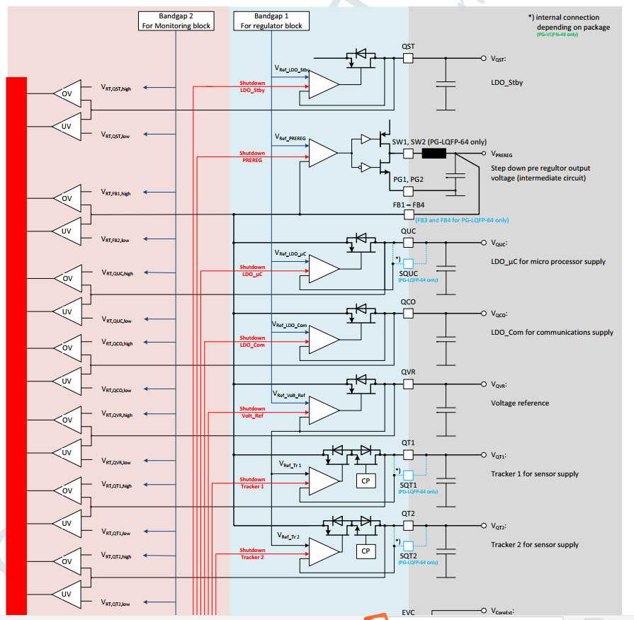
带隙基准和内部电压监控
所有的内部电压也会被监控,如果出现异常会进入POWNDOWN状态。TLF35584包含两路互相独立的带隙基准参考电压互相监控对方的操作。如果超过某一预设的门限值,TLF35584将会产生一个中断给到外部,MCU可以利用这个中断做一些响应。
热关断
TLF35584包含热监控以保护设备在高温条件下损坏,内部有多点的温度保护来防止器件损坏,如果检测到过温,会产生中断给到MCU, MCU应当作出一些反映,如可以关断某路电源输出。
错误管脚监控
TLF35584提供一个可以通过ERR脚监控MCU的安全管理单元SMU,一个预定义的频率范围的翻转方波信号必须给到TLF35584的ERR脚,如果是超过频率范围的信号给到ERR脚会引起报故障,TLF35584将会进入INT状态。默认情况下ERR脚功能是使能的。
窗口看门狗
TLF35584包含一个窗口看门狗来监控MCU的运行,需要一定间隔内收到触发信号,可以通过WDI脚或者SPI,在一定的开窗时间内或者超时触发都会被认为是无效的看门狗触发,无效看门狗触发事件将会引起内部错误计数器加2,并且产生中断,有效的看门狗触发事件将会引起错误计数减1,如果错误计数器超过配置的门限值,TLF35584将会跳转到INT状态。默认条件下窗口看门狗是使能的,需要注意的是窗口看门狗和功能看门狗是相互独立的,可以同时使能使用。
功能看门狗
功能看门狗稍微复杂一些,也叫问答看门狗,通过多个SPI通信帧完成。TLF35584产生一个问题,同时心跳计数器开始从0向上计数,直到心跳周期结束,心跳周期可以通过SPI调整配置,4个字节的响应答案必须在心跳周期结束之前收到。最后一个收到的响应必须同步写入同步寄存器以复位心跳计数器。如果接收到正确的答案响应,认为是一次有效的看门狗触发事件,有效的看门狗触发事件会导致内部错误计数器减1,无效的看门狗触发事件将会导致内部错误计数器加2,并且产生中断。如果错误计数器超过预设的门限值,将会跳转到INT状态。默认情况下功能看门狗是禁止的,和窗口看门狗可以独立使用,互不干涉。
二次安全关断能力
TLF35584具有二次安全关断能力,在应用中安全状态输出引脚SS1和SS2的状态用来表明设备的安全状态。
软错误检测和修正
TLF35584通过一些寄存器提供了软错误的检测和修正安全机制,包括单个位错误的检测和修正,以及两个位错误的检测。两个位错误会引起中断。
安全机制软件需求
TLF35584在安全相关应用中用作微处理器电源。安全机制必须由相应的微处理器执行,以保证系统的正确运行。
SPI通信
来自微处理器的SPI通信用于配置TLF35584,服务看门狗和监控状态寄存器,由于SPI通信是用来传输安全相关信息的,因此需要采取措施保证其数据的完整性
奇偶校验
Assumption: [SM_SPI_01]
SPI通信中的奇偶校验位为每次通信进行检查。具有无效奇偶校验信息的数据必须被忽略。
奇偶校验位在SPI期间防止单比特故障和奇数比特错误的故障沟通。为了提供更全面的误差覆盖范围,可以考虑额外的措施。如果在读操作过程中奇偶校验信息不正确,微处理器必须忽略数据和重做读操作
如果写操作过程中的校验信息不正确,TLF35584将忽略该数据并产生中断。微处理器应该响应中断并检查中断源,即检查是否SPI.PARE位置位。如果写操作失败,微处理器应该重复这个操作。
配置
Assumption: [SM_SPI_02]
write-verify-apply过程用于对安全相关配置的写访问。因此,数据应是在写入数据之后和应用于应用程序之前进行验证。预期配置的验证至少每次配置校验一次,并根据应用程序可以重新配置。
所有与安全相关的配置寄存器(称为“受保护的寄存器”)都由定义的LOCK/UNLOCK过程,允许在数据激活之前对其进行验证。
清除状态和中断寄存器
所有状态和中断标志在清除之前被正确读取。挂起的中断没有正确清除服务
中断信号
Assumption: [SM_INT_01]
根据具体的应用,在将中断信号用作安全功能的应用中,对每个中断信号的正确功能进行验证。
中断的处理,当产生中断,应遵循:
可以实施超时,其到期应视为测试失败。持续时间超时时间应根据所选择的中断源设置
读取中断状态寄存器并验证中断标志是否与生成的特定中断相匹配
中断响应
Assumption: [SM_INT_02]
微处理器检查每个中断事件的中断源,并根据应用程序做出反应要求。
Assumption: [SM_INT_03]
如果通过中断状态标志SYSSF.CFGE检测到一个配置错误,MCU应该对设备进行重新配置
复位输出使用
Assumption: [SM_ROT_01]
TLF35584的复位输出脚ROT连接到MCU的复位输入引脚,当有复位引脚输出,主要安全路径激活。
备用Stand-by LDO使用
Assumption: [SM_SBL_01]
在备用LDO用作微控制器的存储器电源供给时,需要每个周期确认验证下此LDO是否安全。
独立的二次安全关断路径
Assumption: [SM_SS_01]
必须确保主要安全关断路径和二次安全关断路径的独立性,不能存在任何的依赖关系。
一次关断路径或者脚主要关断路径由MCU控制。
Assumption: [SM_SS_02]
在将二次关断路径用作安全功能的应用中,根据不同的应用,要验证其正确的功能,每个周期至少需要一次安全功能验证。
窗口看门狗
Assumption: [SM_WWD_01]
在将窗口看门狗用作安全功能的应用程序中,根据应用至少在每个驾驶周期验证一次窗口看门狗的正确性
Assumption: [SM_WWD_02]
在将窗口看门狗用作安全功能的应用程序中,其正确的功能包括微处理器复位信号ROT和安全状态输出的激活在每个周期至少验证一次。
功能看门狗
Assumption: [SM_FWD_01]
在将功能看门狗用作安全功能的应用中,至少要验证其正确的功能,每个驾驶周期一次,取决于应用程序。
Assumption: [SM_FWD_02]
在功能看门狗作为安全功能发布的应用程序中,其正确的功能包括微处理器复位信号ROT和安全状态输出的激活在每次驾驶中至少验证一次,周期取决于应用程序。
ERR引脚监控
Assumption: [SM_ERR_01]
在将ERR引脚用作安全功能的应用程序中,每次至少验证一次其正确功能,驱动周期取决于应用。
Assumption: [SM_ERR_02]
在ERR引脚用作安全功能的应用中,其正确的功能包括微处理器复位信号ROT和安全状态输出的激活在每个驾驶周期至少验证一次。
请注意,测试程序的可用性取决于错误引脚监控的配置应用:立即行动与恢复延迟
监控组件
Assumption: [SM_MON_01]
在监控块用作安全功能的应用程序中,监视器的正确功能,每个使用的监视器每个驱动周期至少验证一次对中断信号的监控。
Assumption: [SM_MON_02]
在监控块用作安全功能的应用程序中,监视器的正确功能在对每个已使用的监视器至少进行一次验证,以激活安全状态输出周期取决于应用程序。
ABIST
ABIST的检测由MCU发起请求
详细执行规则可以参考SM手册要求,这里不在赘述。
监控功能恢复
如果对设备的监督功能的测试导致异常或失败,则相应的监督功能应被认为是非活性的,并应考虑相应的系统反应以确保安全操作。由于缺乏监督功能并不一定意味着违反了安全目标,微控制器可以控制场景,以增加系统的可用性。进一步讲系统集成者可以预见恢复机制,使监管恢复有效运作。,如可以重新配置有问题的配置,或者重启TLF35584.
硬件需求
二次关断路径
Assumption: [SM_SS_03]
在应用中要确保SS1和SS2的高电平输出被认为是使二次安全关断路径无效,低电平或者高阻态被认为是激活安全关断路径的信号。
Assumption: [SM_SS_04]
SS1和SS2之间的延迟不能被视为安全特性
最大额定值
Assumption: [SM_ABS_01]
在任何操作下都不能违反数据手册中电气参数的最大额定值
电压电流
温度
外部器件的选择
反相保护
因为TLF35584本身不能够处理反相供电的情况,所以需要外部系统层的额外电路来处理电池电压的反接情况。
输入滤波
为了使TLF35584都在额定电气参数范围内操作,强烈建议添加输入滤波器,以限制电源线上的尖峰,相关的参数可以从TLF35584的EMC测试报告中获取。
过流限制
强烈建议在管脚添加限流电阻,防止引脚的电流超过手册的限制值。输入电压VST的限制主要靠前级降压器件来提供可靠输入。如我们的应用中的LM5085.
主要分为两类
一类是连接到电池电压等级的ENA和WAK脚必须小心处理过流和反相,至少大于10K的串联电阻
第二类是像SPI(SCS,SCL,SDI,SDO),INT,ROT,WDI,SYN,EVC 至少串联一个大于50欧姆的电阻,电阻布局的位置也需在系统级考虑。
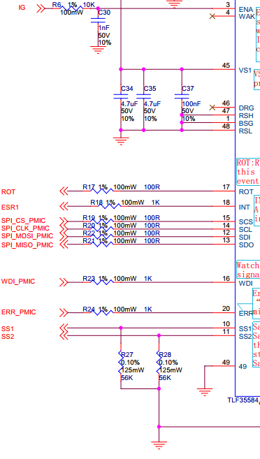
ERR脚保护
在MCU的SMU故障输出脚P33.8和TLF35584的ERR脚之间串联大于1K的电阻。

电压域的分离
强烈建议将ECU内的高、低压区分开,在不同组的信号之间的电路以减少短路的风险。这可以通过在PCB布线中使用足够的间隙来完成任何外部高压和内部低压信号之间。在这种情况下应给予特别考虑不同域的信号在引脚上连接。
外部被动元器件
必须强制确保连接到TLF35584的外部器件在数据手册要求的范围内,如输出电感,电容等。外部器件组件的失效必须在系统层级覆盖,可以使用冗余外部器件,提高系统层级的可靠性。可以参考数据手册有关外部器件要求更详细的信息,这里只给出简单的要求
总结:
要根据自己的应用选择内外安全机制去执行,提高系统的安全。
审核编辑:刘清
-
英飞凌
+关注
关注
68文章
2563浏览量
143174 -
看门狗
+关注
关注
10文章
611浏览量
73200 -
电源管理
+关注
关注
117文章
8653浏览量
148249 -
电源管理芯片
+关注
关注
23文章
1004浏览量
55799 -
SPI通信
+关注
关注
0文章
41浏览量
12011 -
中断响应
+关注
关注
0文章
11浏览量
3256 -
TLF35584
+关注
关注
0文章
2浏览量
6150
原文标题:英飞凌电源管理PMIC的安全应用
文章出处:【微信号:InterruptISR,微信公众号:嵌入式程序员】欢迎添加关注!文章转载请注明出处。
发布评论请先 登录
请问TC397 PMIC TLF35584看门狗在正常情况下没有喂狗,会让它重置信号吗?
TLF35584将MCU电源连接到QUC,如果QUC处于低电平状态,则MCU会死机怎么解决?
TLF35584 Aurix-CompanionBoard插上microUSB线缆时无法连接是为什么?
TC375在TLF35584处于待机状态时硬重置是怎么回事?
使用TLF35584来控制TC397,ROT引脚总是很高怎么解决?
SCR模式下如何通过TC397唤醒TLF35584进入NORMAL模式?
TLF35584后置稳压器ldo_μc的输出电压是不是可以修改?
在什么情况下TLF35584的输出电压VQUC会发生压力或压强呢?
请问如何重置TLF35584?
如何在TC387中禁用35584的MPS?
分功率板和控制板但是可以整合在一起的BMS的产品
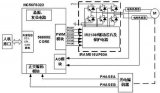
电机控制器在电动汽车中的位置和作用


评论