 如何对MAX22000可配置模拟IO进行编程

MAX22000为可配置模拟IO器件。它支持1通道通用电压/电流输入输出(IO)以及RTD或热电偶输入作为行业标准4端子接口。或者,它可用于创建双通道差分模拟输入或六通道单端模拟输入。微控制器兼容型串行外设接口(SPI)提供对许多高级功能的访问。本应用笔记提供了C代码实现示例,包括设置、监控和诊断功能。
介绍
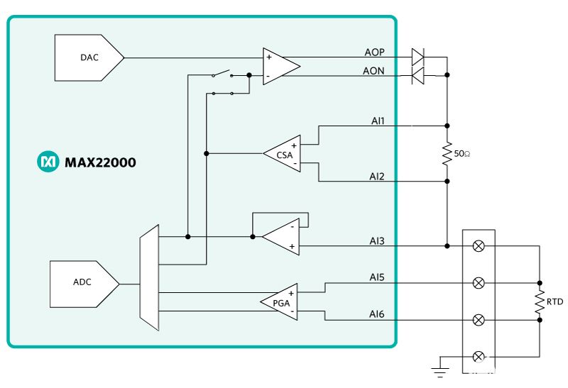
MAX22000集成了24位ADC、18位DAC和模拟前端(AFE),可创建软件可配置IO,支持所有标准工业模拟接口:-10V至+10V模拟输入或输出、-20mA至+20mA模拟输入或输出,以及用于温度测量的RTD或热电偶输入。当用作模拟输入 (AI) 时,该器件支持具有两个单端输入的差分输入通道或多达六个单端输入通道。此外,一个差分输入通道(AI5和AI6)具有集成的低噪声可编程增益放大器(PGA),专为热电偶或RTD测量而设计。
如果使用模拟输出(AO),则在电流输出模式下需要一个差分模拟输入对,或者在电压输出模式下需要一个单端模拟输入通道。
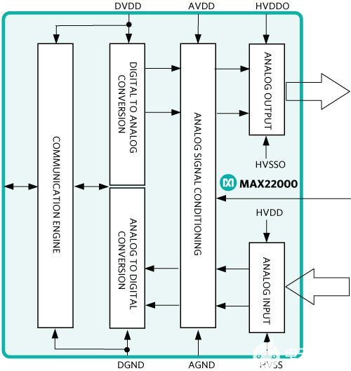
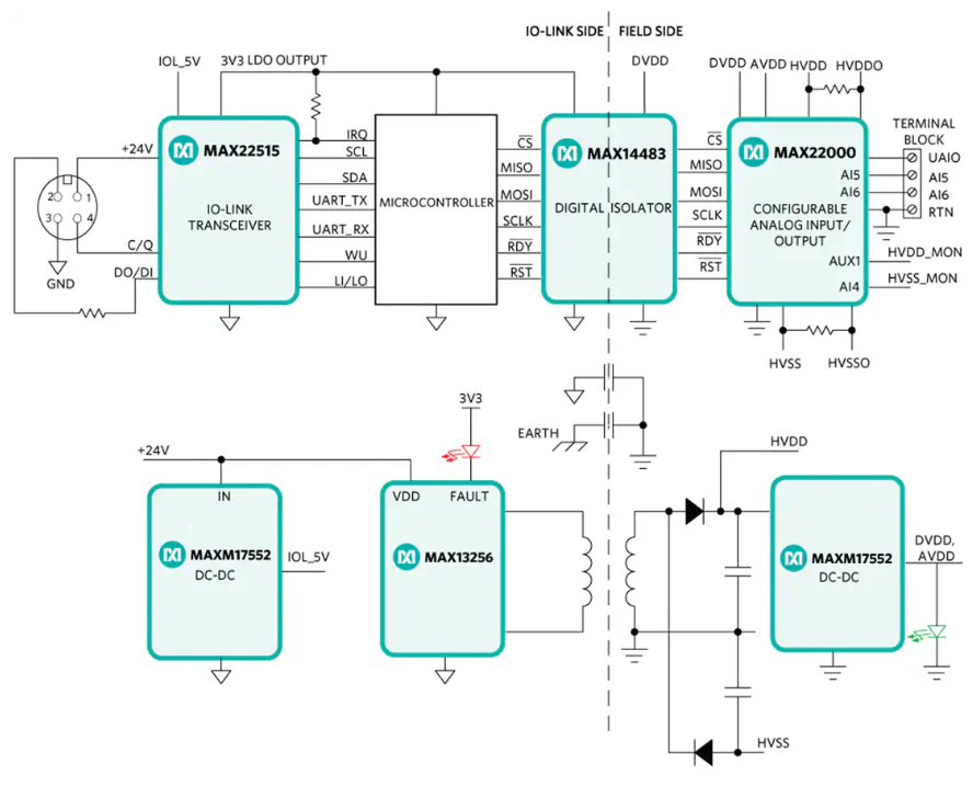
本应用笔记介绍了一系列功能,为MAX22000编程提供更快、经过验证的解决方案(图1)。它们是用C语言编写的,应该很容易移植到任何常见的微控制器上。有关MAX22000引脚、工作模式和控制寄存器的详细信息,请参考MAX22000数据资料。
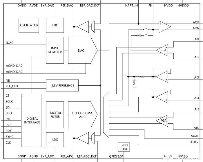
图1.MAX22000功能框图
MAX22000 SPI
MAX22000 SPI命令为32位长(8位指令+24位数据),CRC禁用,如果使能CRC,则CRC8将增加8位;有关CRC计算的详细信息,请参见应用笔记7072:MAX22000可配置模拟IO的CRC编程指南,其中更详细地显示了CRC8编码。SPI 命令结构如表 1所示。MAX22000的SPI模式为CPOL = 0 (CLK空闲= 0),CPHA = 0 (上升沿/第一沿对数据进行采样),数据/命令需要先以MSB时钟。
表 1.MAX22000 SPI命令结构
| 地址 | 控制 | 数据 |
|---|---|---|
| 7 位 A[6:0],MSB 至 LSB | R/W 位,读取 = 1,写入 = 0 | 24 位 D[23:0],MSB 至 LSB |
有关SPI读写周期的详细信息,以及寄存器表和指令,请参见MAX22000数据资料。
图1所示为MAX22000的主要功能块。从本质上讲,该设备有四个主要部分:
带有内部基准电压源的Σ-Δ型ADC – 主要功能是转换可使用SPI读取的模拟数据。
带内部基准电压源的DAC – 主要功能是将数字数据转换为模拟电压。
带多路复用器的AFE – 主要功能是选择通道和开关模式(即电流/电压)。
逻辑端接口 – SPI 端口,用于访问所有器件寄存器和硬件标志以进行诊断。
MAX22000—应用示例 可配置的多量程模拟输入/输出
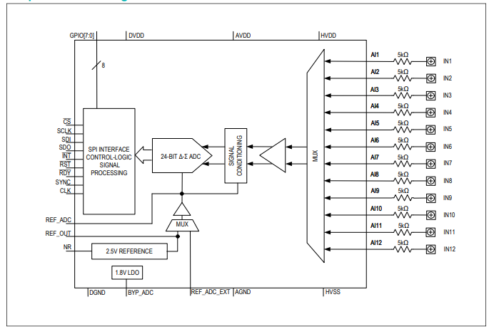
MAX22000设计用于支持终端设备的工业应用,如需要可配置模拟I/O的可编程逻辑控制器(PLC)。典型应用电路如图2所示。
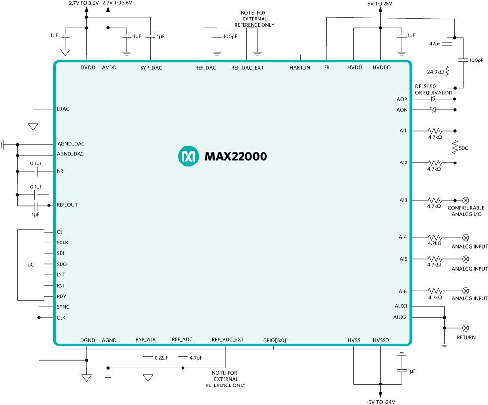
图2.可配置模拟 IO + 3 个单端模拟电压输入。
标有“通用模拟 I/O”的终端是软件可配置且完全灵活的模拟 IO 端口,与标有“Return”的终端一起提供:
电流输入±20mA (标称)满量程范围为±25mA。
电流输出±20mA (标称)满量程范围为±25mA。
电压输入±10V(标称),满量程范围为±12.5V。
电压输出±10V(标称),满量程范围为±12.5V。
为了简化需要电流隔离的系统,MAX22000支持6个逻辑电平GPIO(GPIO[5:0]),可用于需要切换外部元件(MUX/FET/电源)或需要通过隔离栅回读数字信号的情况。
源代码
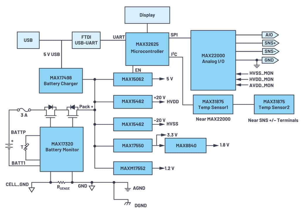
本应用笔记提供了C源代码示例,主要提供驱动器功能,用于访问MAX22000中的多个寄存器,以实现配置、控制和诊断功能。所有软件均使用MAX22000评估板进行实现和测试。
全局允许轻松选择通道/模式:
public enum Register_address
{
GEN_PROD = 0x00,
GEN_REV = 0x01,
GEN_CNFG = 0x02,
GEN_CHNL_CTRL = 0x03,
GEN_GPIO_CTRL = 0x04,
GEN_GPI_INT = 0x05,
GEN_GPI_DATA = 0x06,
GEN_INT = 0x07,
GEN_INTEN = 0x08,
GEN_PWR_CTRL = 0x09,
GEN_TST_MODE_1 = 0x1a,
GEN_TST_ENTRY = 0x1c,
GEN_TST69 = 0x1d,
DCHNL_CMD = 0x20,
DCHNL_STA = 0x21,
DCHNL_CTRL1 = 0x22,
DCHNL_CTRL2 = 0x23,
DCHNL_DATA = 0x24,
DCHNL_N_SEL = 0x25,
DCHNL_N_SOC = 0x26,
DCHNL_N_SGC = 0x27,
AO_DATA_WR = 0x40,
AO_OFFSET_CORR_WR = 0x41,
AO_GAIN_CORR_WR = 0x42,
AO_CNFG_WR = 0x43,
AO_DATA_RD = 0x44,
AO_OFFSET_CORR_RD = 0x45,
AO_GAIN_CORR_RD = 0x46,
AO_STA_RD = 0x47,
};
// DAC is 18bit, full-range = 262144; Half because bipolar: 131072, Theoretical factor = V(range) / half-range
public const double phy_AO_25V_factor = (double) 25 / (double) 262144; //0.00009536743164;
public const double phy_AO_25V_offset = -131072;
public const double phy_AO_12V_factor = (double) 25 / (double) 262144; //0.00009536743164;
public const double phy_AO_12V_offset = 0;
// DAC is 18bit, full-range = 262144; Theoretical factor = mA(range) / half-range (bipolar)
public const double phy_AO_25mA_factor = (double) 50 / (double) 262144; // 0.0001907348633;
public const double phy_AO_25mA_offset = 0;
public const double phy_AO_2mA_factor = (double) 5 / (double) 262144; // 0.00001907348633;
public const double phy_AO_2mA_offset = 0;
public enum Channel_select
{
AI1_SE_b12V = 0x00,
AI2_SE_b12V = 0x01,
AI1_2_diff_b1V = 0x02,
AI3_SE_b12V = 0x03,
AI4_SE_b12V = 0x04,
AI3_4_diff_b25V = 0x05,
AI5_SE_b12V = 0x06,
AI6_SE_b12V = 0x07,
AI5_6_diff_b25V = 0x08,
AI5_SE_b0p125V = 0x09,
AI5_SE_b0p250V = 0x0a,
AI5_SE_b0p500V = 0x0b,
AI5_SE_b2p500V = 0x0c,
AI6_SE_b0p125V = 0x0d,
AI6_SE_b0p250V = 0x0e,
AI6_SE_b0p500V = 0x0f,
AI6_SE_b2p500V = 0x10,
AI5_6_diff_b0p125V = 0x11,
AI5_6_diff_b0p250V = 0x12,
AI5_6_diff_b0p500V = 0x13,
AI5_6_diff_b2p500V = 0x14,
AUX1_SE_u2V = 0x15,
AUX2_SE_u2V = 0x16,
AUX1_2_diff_b2V = 0x17,
};
public enum AOut_Mode
{
high_impedance = 0,
AO_25V = 1,
AO_12V = 2,
AO_6V = 3,
AO_1V = 4,
AO_0p6V = 5,
AO_25mA = 6,
AO_12mA = 7,
AO_2mA = 8,
AO_1mA = 9,
out_of_range1 = 10
}
public enum MAX22000_CIO_Mode
{
Current_Input,
Voltage_Input,
Current_Output,
Voltage_Output,
RTD_Input,
PGA_Input,
PGA_Input_with_Current_sourcing,
Off
};
//********************************************************************
//*
//* Function: MAX22000_read_register
//* Description: Read one Register from MAX22000
//*
//* Input: Register-Address (take from definitions in header-file)
//* Output: 24bit register content
//*
//* if CRC is enabled, then crc8-Command is required
//*
//********************************************************************/
public UInt32 MAX22000EVKIT_read_register(Register_address address)
{
UInt32 result = 0;
UInt32 CRC_read = 0;
if (CRC_Enabled == false)
{
max22000_port.SPI_CS0Enable();
max22000_port.SPI_W_transaction_8( (address << 1) + 0x01 );
result = max22000_port.SPI_R_transaction_24();
max22000_port.SPI_CS0Disable();
}
else
{
max22000_port.SPI_CS0Enable();
max22000_port.SPI_W_transaction_8( (address << 1) + 0x01 );
result = max22000_port.SPI_R_transaction_24();
CRC_read = max22000_port.SPI_R_transaction_8(); // read the CRC
max22000_port.SPI_CS0Disable();
// calculate and check...
byte CRC_TX1 = (address << 1) + 0x01; // TX byte (was sent)
byte CRC_RX1 = (result >>16) & 0xff; // 1st RX byte
byte CRC_RX2 = (result >>8 ) & 0xff; // 2nd RX byte
byte CRC_RX3 = (result ) & 0xff; // 3rd RX byte
byte CRC_Calc = crc8(CRC_TX1, CRC_RX1, CRC_RX2, CRC_RX3);
if (CRC_Calc != CRC_read) printf("CRC read from MAX22000 is incorrect.");
}
return result;
}
//********************************************************************
//*
//* Function: MAX22000_write_register
//* Description: Write one Register to MAX22000
//*
//* Input: Register-Address (take from definitions in header-file)
//* 24bit data (new register content)
//*
//********************************************************************/
public UInt32 MAX22000EVKIT_write_register(Register_address address, UInt32 data)
{
if (CRC_Enabled == false)
{
max22000_port.SPI_CS0Enable();
max22000_port.SPI_W_transaction_8( (ushort) ( ((byte)address << 1) ) );
max22000_port.SPI_W_transaction_24(data);
max22000_port.SPI_CS0Disable();
}
else
{
byte CRC_TX1 = (address << 1);
byte CRC_TX2 = ((data> >16) & 0xff);
byte CRC_TX3 = ((data >>8 ) & 0xff);
byte CRC_TX4 = ( data & 0xff);
byte CRC_Calc = crc8(CRC_TX1, CRC_TX2, CRC_TX3, CRC_TX4);
max22000_port.SPI_CS0Enable();
max22000_port.SPI_W_transaction_8( address << 1 );
max22000_port.SPI_W_transaction_24(data);
max22000_port.SPI_W_transaction_8( CRC_Calc );
max22000_port.SPI_CS0Disable();
}
}
// ********************************************************************
//
// Function: MAX22000_CIO_Setup
// Description: Sets up MAX22000 for one of the CIO Modes
// Assuming HW is connected like the standard application diagram
//
// Input: Desired Mode
// Output: None (MAX22000 will be setup by this routine)
//
// ********************************************************************
uint32_t MAX22000_CIO_Setup (MAX22000_CIO_Mode mode)
{
uint32_t ADC_result = 0;
switch (mode)
{
case MAX22000_CIO_Mode.Current_Input:
// set calibration factors for Current Input
MAX22000_write_register(MAX22000_DCHNL_CMD, 0x100000); // Stop any potentially running conversions
MAX22000_write_register(MAX22000_GEN_CHNL_CTRL, 0x000000); // No channel selected
MAX22000_write_register(MAX22000_DCHNL_N_SEL, 0x000003); // Select CH AI1-2 diff calibration factor
MAX22000_write_register(MAX22000_DCHNL_N_SOC, 0xFFFFE1); // Write Offset (regular low-side)
MAX22000_write_register(MAX22000_DCHNL_N_SGC, 0xBD934B); // Write Gain (regular low-side)
// END restore calibration
uint32_t new_GEN_CNFG = 0;
new_GEN_CNFG = (new_GEN_CNFG & 0xff1fff) + 0x008000; // AI1-2 diff (CSA-Mode)
new_GEN_CNFG = (new_GEN_CNFG & 0xf0ffff) + 0x020000; // AO voltage output mode +/- 12.5V range
MAX22000_write_register(MAX22000_GEN_CNFG, new_GEN_CNFG); // Write new_GEN_CNFG_value
MAX22000_write_register(MAX22000_AO_DATA_WR, 0x000000); // Write AO Voltage to 0V so current can flow
// Prepare ADC
MAX22000_write_register(MAX22000_GEN_CHNL_CTRL, 0x000300); // AI1-2 diff channel selected
MAX22000_write_register(MAX22000_DCHNL_CTRL1, 0x010000); // Continuous Single cycle conversions
MAX22000_write_register(MAX22000_DCHNL_CTRL2, 0x000000); // Internal OSC, use coefficients, ...
MAX22000_write_register(MAX22000_GEN_CHNL_CTRL, 0x000300); // select AI1-2 diff mode
MAX22000_write_register(MAX22000_DCHNL_CMD, 0x310000); // Start conversion (10sps) (0x340000 = 50sps)
ADC_result = MAX22000EVKIT_read_register(MAX22000_DCHNL_DATA);// read Data
break;
case MAX22000_CIO_Mode.Current_Output:
// Set DAC calibration
MAX22000_write_register(MAX22000_AO_OFFSET_CORR_WR, 0x00F5C0);
MAX22000_write_register(MAX22000_AO_GAIN_CORR_WR, 0xFA3E80);
// END restore calibration
// Set AO Mode (Register 0x02: GEN_CNFG)
uint32_t new_GEN_CNFG = 0;
new_GEN_CNFG = (new_GEN_CNFG & 0xff1fff) + 0x008000; // AI1-2 diff (CSA-Mode)
new_GEN_CNFG = (new_GEN_CNFG & 0xf0ffff) + 0x060000; // AO current output mode +/- 25mA range
new_GEN_CNFG = (new_GEN_CNFG & 0xeFffff) + 0x000000; // Set 4-wire Mode
new_GEN_CNFG = (new_GEN_CNFG & 0xffefff) + 0x001000; // enable AI3 SE
new_GEN_CNFG = (new_GEN_CNFG & 0xbfffff) + 0x000000; // Internal Reference
MAX22000_write_register(MAX22000_GEN_CNFG, new_GEN_CNFG); // Write new_GEN_CNFG_value
MAX22000_write_register(MAX22000_GEN_PWR_CTRL, 0x000000); // Normal operation (especially make sure GEN_PD=0
// Set Hex value / physical Value
MAX22000_write_register(MAX22000_AO_DATA_WR, 0);//new_AO_value<<6); // Write new DAC value
break;
case MAX22000_CIO_Mode.Voltage_Input:
// restore calibration
MAX22000_write_register(MAX22000_DCHNL_CMD, 0x100000); // Stop any potentially running conversions
MAX22000_write_register(MAX22000_GEN_CHNL_CTRL, 0x000000); // No channel selected
MAX22000_write_register(MAX22000_DCHNL_N_SEL, 0x000003); // Select CH AI3 SE calibration factor
MAX22000_write_register(MAX22000_DCHNL_N_SOC, 0xFFFFE1); // Write Offset
MAX22000_write_register(MAX22000_DCHNL_N_SGC, 0xBD934B); // Write Gain
// END restore calibration
uint32_t new_GEN_CNFG = 0;
new_GEN_CNFG = (new_GEN_CNFG & 0xffefff) + 0x001000; // AI3 SE enabled
new_GEN_CNFG = (new_GEN_CNFG & 0xf0ffff) + 0x000000; // AO High-Impedance mode
new_GEN_CNFG = (new_GEN_CNFG & 0xeFffff) + 0x000000; // Set 4-wire Mode
new_GEN_CNFG = (new_GEN_CNFG & 0xbfffff) + 0x000000; // Internal Reference
MAX22000_write_register(MAX22000_GEN_CNFG, new_GEN_CNFG); // Write new_GEN_CNFG_value
// Select Internal REFs, set all channels to single-ended leave as is
MAX22000_write_register(MAX22000_DCHNL_CTRL1, 0x010000); // Continuous Single cycle conversions
MAX22000_write_register(MAX22000_DCHNL_CTRL2, 0x000000); // Internal OSC, use coefficients, ...
MAX22000_write_register(MAX22000_GEN_CHNL_CTRL, 0x000400); // Select Channel AI3 / Single Ended
//MAX22000_write_register(MAX22000_DCHNL_CMD, 0x330000); // Start conversion (30sps)
MAX22000_write_register(MAX22000_DCHNL_CMD, 0x310000); // Start conversion (10sps)
break;
case MAX22000_CIO_Mode.Voltage_Output:
MAX22000_write_register(MAX22000_AO_OFFSET_CORR_WR, 0x00F5C0);
MAX22000_write_register(MAX22000_AO_GAIN_CORR_WR, 0xFA3E80);
// END restore calibration
uint32_t new_GEN_CNFG = 0;
new_GEN_CNFG = (new_GEN_CNFG & 0xf0ffff) + 0x020000; // 10V is 0b0010 -> 2
new_GEN_CNFG = (new_GEN_CNFG & 0xeFffff) + 0x000000; // Set 4-wire Mode
new_GEN_CNFG = (new_GEN_CNFG & 0xbfffff) + 0x000000; // Internal Reference
MAX22000_write_register(MAX22000_GEN_CNFG, new_GEN_CNFG); // Write new_GEN_CNFG_value
// Set Hex value / physical Value
MAX22000_write_register(MAX22000_AO_DATA_WR, 0);//new_AO_value<<6); // Write new DAC value
break;
case MAX22000_CIO_Mode.Off:
// Make AO high-impedance, Stop ADC, Disable all Amplifiers
MAX22000_write_register(MAX22000_DCHNL_CMD, 0x100000); // Stop any potentially running conversions
MAX22000_write_register(MAX22000_GEN_CHNL_CTRL, 0x000000); // No channel selected
MAX22000_write_register(MAX22000_GEN_CNFG, 0x000000); // Write new_GEN_CNFG_value
break;
case default:
// Make AO high-impedance, Stop ADC, Disable all Amplifiers
MAX22000_write_register(MAX22000_DCHNL_CMD, 0x100000); // Stop any potentially running conversions
MAX22000_write_register(MAX22000_GEN_CHNL_CTRL, 0x000000); // No channel selected
MAX22000_write_register(MAX22000_GEN_CNFG, 0x000000); // Write new_GEN_CNFG_value
break;
}
}
// ********************************************************************
//
// Function: MAX22000_ADC_Setup
// Description: Sets up MAX22000 for to read one of the ADC Channels in selected Mode
// Assuming all ADCs (at least the selected one) is open / connected to a voltage source
//
// Input: Desired ADC-Channel +Mode
// Output: None (MAX22000 will be setup by this routine, Conversion will be started)
//
// ********************************************************************
uint32_t MAX22000_ADC_Setup (ADC_CH_Mode CH_and_Mode)
{
switch(CH_and_Mode)
{
case ADC_CH_Mode.AI1_SE:
// Setup Channel 1 for Single Ended and continuous sampling
uint32_t new_GEN_CNFG = 0;
new_GEN_CNFG = (new_GEN_CNFG & 0xff1fff) + 0x006000; // make AI1 and AI2 SE active
MAX22000_write_register(MAX22000_GEN_CNFG, new_GEN_CNFG); // Write new_GEN_CNFG_value
// Select Internal REFs, set all channels to single-ended leave as is
MAX22000_write_register(MAX22000_DCHNL_CTRL1, 0x010000); // Continuous Single cycle conversions
MAX22000_write_register(MAX22000_DCHNL_CTRL2, 0x000000); // Internal OSC, use coefficients, ...
MAX22000_write_register(MAX22000_GEN_CHNL_CTRL, 0x000100); // Select Channel AI1 / Single Ended
//MAX22000_write_register(MAX22000_DCHNL_CMD, 0x330000); // Start conversion (30sps)
MAX22000_write_register(MAX22000_DCHNL_CMD, 0x310000); // Start conversion (10sps)
break;
case ADC_CH_Mode.AI2_SE:
// Setup Channel 2 for Single Ended and continuous sampling
uint32_t new_GEN_CNFG = 0;
new_GEN_CNFG = (new_GEN_CNFG & 0xff1fff) + 0x006000; // make AI1 and AI2 SE active
MAX22000_write_register(MAX22000_GEN_CNFG, new_GEN_CNFG); // Write new_GEN_CNFG_value
// Select Internal REFs, set all channels to single-ended leave as is
MAX22000_write_register(MAX22000_DCHNL_CTRL1, 0x010000); // Continuous Single cycle conversions
MAX22000_write_register(MAX22000_DCHNL_CTRL2, 0x000000); // Internal OSC, use coefficients, ...
MAX22000_write_register(MAX22000_GEN_CHNL_CTRL, 0x000200); // Select Channel AI1 / Single Ended
//MAX22000_write_register(MAX22000_DCHNL_CMD, 0x330000); // Start conversion (30sps)
MAX22000_write_register(MAX22000_DCHNL_CMD, 0x310000); // Start conversion (10sps)
break;
case ADC_CH_Mode.AI3_SE:
// Setup Channel 3 for Single Ended and continuous sampling
uint32_t new_GEN_CNFG = 0;
new_GEN_CNFG = (new_GEN_CNFG & 0xff1fff) + 0x001800; // make AI3 and AI4 SE active
MAX22000_write_register(MAX22000_GEN_CNFG, new_GEN_CNFG); // Write new_GEN_CNFG_value
// Select Internal REFs, set all channels to single-ended leave as is
MAX22000_write_register(MAX22000_DCHNL_CTRL1, 0x010000); // Continuous Single cycle conversions
MAX22000_write_register(MAX22000_DCHNL_CTRL2, 0x000000); // Internal OSC, use coefficients, ...
MAX22000_write_register(MAX22000_GEN_CHNL_CTRL, 0x000400); // Select Channel AI3 / Single Ended
//MAX22000_write_register(MAX22000_DCHNL_CMD, 0x330000); // Start conversion (30sps)
MAX22000_write_register(MAX22000_DCHNL_CMD, 0x310000); // Start conversion (10sps)
break;
case ADC_CH_Mode.AI4_SE:
// Setup Channel 4 for Single Ended and continuous sampling
uint32_t new_GEN_CNFG = 0;
new_GEN_CNFG = (new_GEN_CNFG & 0xff1fff) + 0x000800; // make AI4 SE active
MAX22000_write_register(MAX22000_GEN_CNFG, new_GEN_CNFG); // Write new_GEN_CNFG_value
// Select Internal REFs, set all channels to single-ended leave as is
MAX22000_write_register(MAX22000_DCHNL_CTRL1, 0x010000); // Continuous Single cycle conversions
MAX22000_write_register(MAX22000_DCHNL_CTRL2, 0x000000); // Internal OSC, use coefficients, ...
MAX22000_write_register(MAX22000_GEN_CHNL_CTRL, 0x000500); // Select Channel AI4 / Single Ended
//MAX22000_write_register(MAX22000_DCHNL_CMD, 0x330000); // Start conversion (30sps)
MAX22000_write_register(MAX22000_DCHNL_CMD, 0x310000); // Start conversion (10sps)
break;
case ADC_CH_Mode.AI12_DIFF:
// Setup Channel 1-2 for Differeential and continuous sampling
uint32_t new_GEN_CNFG = 0;
new_GEN_CNFG = (new_GEN_CNFG & 0xff1fff) + 0x008000; // enable AI1-2 diff (CSA) mode
MAX22000_write_register(MAX22000_GEN_CNFG, new_GEN_CNFG); // Write new_GEN_CNFG_value
// Select Internal REFs, set all channels to single-ended leave as is
MAX22000_write_register(MAX22000_DCHNL_CTRL1, 0x010000); // Continuous Single cycle conversions
MAX22000_write_register(MAX22000_DCHNL_CTRL2, 0x000000); // Internal OSC, use coefficients, ...
MAX22000_write_register(MAX22000_GEN_CHNL_CTRL, 0x000300); // Select Channel AI1-2 / Differential
//MAX22000_write_register(MAX22000_DCHNL_CMD, 0x330000); // Start conversion (30sps)
MAX22000_write_register(MAX22000_DCHNL_CMD, 0x310000); // Start conversion (10sps)
break;
case ADC_CH_Mode.AI34_DIFF:
// Setup Channel 3-4 for Differeential and continuous sampling
uint32_t new_GEN_CNFG = 0;
new_GEN_CNFG = (new_GEN_CNFG & 0xff1fff) + 0x001800; // enable AI3-AI4 diff
MAX22000_write_register(MAX22000_GEN_CNFG, new_GEN_CNFG); // Write new_GEN_CNFG_value
// Select Internal REFs, set all channels to single-ended leave as is
MAX22000_write_register(MAX22000_DCHNL_CTRL1, 0x010000); // Continuous Single cycle conversions
MAX22000_write_register(MAX22000_DCHNL_CTRL2, 0x000000); // Internal OSC, use coefficients, ...
MAX22000_write_register(MAX22000_GEN_CHNL_CTRL, 0x000600); // Select Channel AI3-4 / Differential
//MAX22000_write_register(MAX22000_DCHNL_CMD, 0x330000); // Start conversion (30sps)
MAX22000_write_register(MAX22000_DCHNL_CMD, 0x310000); // Start conversion (10sps)
break;
case ADC_CH_Mode.AI56_DIFF:
// Setup Channel 5-6 for Differeential and continuous sampling
uint32_t new_GEN_CNFG = 0;
new_GEN_CNFG = (new_GEN_CNFG & 0xff1fff) + 0x000400; // enable AI5-6 diff +/- 25V range
MAX22000_write_register(MAX22000_GEN_CNFG, new_GEN_CNFG); // Write new_GEN_CNFG_value
// Select Internal REFs, set all channels to single-ended leave as is
MAX22000_write_register(MAX22000_DCHNL_CTRL1, 0x010000); // Continuous Single cycle conversions
MAX22000_write_register(MAX22000_DCHNL_CTRL2, 0x000000); // Internal OSC, use coefficients, ...
MAX22000_write_register(MAX22000_GEN_CHNL_CTRL, 0x000900);// Select Channel AI5-6 / Differential +/-25V
//MAX22000_write_register(MAX22000_DCHNL_CMD, 0x330000); // Start conversion (30sps)
MAX22000_write_register(MAX22000_DCHNL_CMD, 0x310000); // Start conversion (10sps)
break;
case ADC_CH_Mode.AI56_PGA_2p500V:
// Setup Channel 5-6 for Differeential and continuous sampling (PGA Path +/-2.5V range)
uint32_t new_GEN_CNFG = 0;
new_GEN_CNFG = (new_GEN_CNFG & 0xff1fff) + 0x000400; // enable AI5-6 diff +/- 2.5V range (in PGA Mode)
MAX22000_write_register(MAX22000_GEN_CNFG, new_GEN_CNFG); // Write new_GEN_CNFG_value
// Select Internal REFs, set all channels to single-ended leave as is
MAX22000_write_register(MAX22000_DCHNL_CTRL1, 0x010000); // Continuous Single cycle conversions
MAX22000_write_register(MAX22000_DCHNL_CTRL2, 0x000000); // Internal OSC, use coefficients, ...
MAX22000_write_register(MAX22000_GEN_CHNL_CTRL, 0x000c00); // Select Channel AI5-6 / Differential PGA Path
//MAX22000_write_register(MAX22000_DCHNL_CMD, 0x330000); // Start conversion (30sps)
MAX22000_write_register(MAX22000_DCHNL_CMD, 0x310000); // Start conversion (10sps)
break;
case ADC_CH_Mode.AI56_PGA_0p500V:
// Setup Channel 5-6 for Differeential and continuous sampling (PGA Path +/-0.5V range)
uint32_t new_GEN_CNFG = 0;
new_GEN_CNFG = (new_GEN_CNFG & 0xff1fff) + 0x000440; // enable AI5-6 diff +/- 0.5V range
MAX22000_write_register(MAX22000_GEN_CNFG, new_GEN_CNFG); // Write new_GEN_CNFG_value
// Select Internal REFs, set all channels to single-ended leave as is
MAX22000_write_register(MAX22000_DCHNL_CTRL1, 0x010000); // Continuous Single cycle conversions
MAX22000_write_register(MAX22000_DCHNL_CTRL2, 0x000000); // Internal OSC, use coefficients, ...
MAX22000_write_register(MAX22000_GEN_CHNL_CTRL, 0x000c00); // Select Channel AI5-6 / Differential PGA Path
//MAX22000_write_register(MAX22000_DCHNL_CMD, 0x330000); // Start conversion (30sps)
MAX22000_write_register(MAX22000_DCHNL_CMD, 0x310000); // Start conversion (10sps)
break;
case ADC_CH_Mode.AI56_PGA_0p250V:
// Setup Channel 5-6 for Differeential and continuous sampling (PGA Path +/-0.250V range)
uint32_t new_GEN_CNFG = 0;
new_GEN_CNFG = (new_GEN_CNFG & 0xff1fff) + 0x000480; // enable AI5-6 diff +/- 0.250V range
MAX22000_write_register(MAX22000_GEN_CNFG, new_GEN_CNFG); // Write new_GEN_CNFG_value
// Select Internal REFs, set all channels to single-ended leave as is
MAX22000_write_register(MAX22000_DCHNL_CTRL1, 0x010000); // Continuous Single cycle conversions
MAX22000_write_register(MAX22000_DCHNL_CTRL2, 0x000000); // Internal OSC, use coefficients, ...
MAX22000_write_register(MAX22000_GEN_CHNL_CTRL, 0x000c00); // Select Channel AI5-6 / Differential PGA Path
//MAX22000_write_register(MAX22000_DCHNL_CMD, 0x330000); // Start conversion (30sps)
MAX22000_write_register(MAX22000_DCHNL_CMD, 0x310000); // Start conversion (10sps)
break;
case ADC_CH_Mode.AI56_PGA_0p125V:
// Setup Channel 5-6 for Differeential and continuous sampling (PGA Path +/-0.250V range)
uint32_t new_GEN_CNFG = 0;
new_GEN_CNFG = (new_GEN_CNFG & 0xff1fff) + 0x0004c0; // enable AI5-6 diff +/- 0.125V range
MAX22000_write_register(MAX22000_GEN_CNFG, new_GEN_CNFG); // Write new_GEN_CNFG_value
// Select Internal REFs, set all channels to single-ended leave as is
MAX22000_write_register(MAX22000_DCHNL_CTRL1, 0x010000); // Continuous Single cycle conversions
MAX22000_write_register(MAX22000_DCHNL_CTRL2, 0x000000); // Internal OSC, use coefficients, ...
MAX22000_write_register(MAX22000_GEN_CHNL_CTRL, 0x000c00); // Select Channel AI5-6 / Differential PGA Path
//MAX22000_write_register(MAX22000_DCHNL_CMD, 0x330000); // Start conversion (30sps)
MAX22000_write_register(MAX22000_DCHNL_CMD, 0x310000); // Start conversion (10sps)
break;
case ADC_CH_Mode.AUX1_SE:
// Setup Channel AUX1 for Single Ended and continuous sampling
// Select Internal REFs, set all channels to single-ended leave as is
MAX22000_write_register(MAX22000_DCHNL_CTRL1, 0x010000); // Continuous Single cycle conversions
MAX22000_write_register(MAX22000_DCHNL_CTRL2, 0x000000); // Internal OSC, use coefficients, ...
MAX22000_write_register(MAX22000_GEN_CHNL_CTRL, 0x000d00); // Select Channel AUX1 / Single Ended
//MAX22000_write_register(MAX22000_DCHNL_CMD, 0x330000); // Start conversion (30sps)
MAX22000_write_register(MAX22000_DCHNL_CMD, 0x310000); // Start conversion (10sps)
break;
case ADC_CH_Mode.AUX2_SE:
// Setup Channel AUX2 for Single Ended and continuous sampling
// Select Internal REFs, set all channels to single-ended leave as is
MAX22000_write_register(MAX22000_DCHNL_CTRL1, 0x010000); // Continuous Single cycle conversions
MAX22000_write_register(MAX22000_DCHNL_CTRL2, 0x000000); // Internal OSC, use coefficients, ...
MAX22000_write_register(MAX22000_GEN_CHNL_CTRL, 0x000e00); // Select Channel AUX2 / Single Ended
//MAX22000_write_register(MAX22000_DCHNL_CMD, 0x330000); // Start conversion (30sps)
MAX22000_write_register(MAX22000_DCHNL_CMD, 0x310000); // Start conversion (10sps)
break;
case ADC_CH_Mode.AUX12_DIFF:
// Setup Channel AUX1-2 for Differential and continuous sampling
// Select Internal REFs, set all channels to single-ended leave as is
MAX22000_write_register(MAX22000_DCHNL_CTRL1, 0x010000); // Continuous Single cycle conversions
MAX22000_write_register(MAX22000_DCHNL_CTRL2, 0x000000); // Internal OSC, use coefficients, ...
MAX22000_write_register(MAX22000_GEN_CHNL_CTRL, 0x000f00); // Select Channel AUX1-2 / Differential
//MAX22000_write_register(MAX22000_DCHNL_CMD, 0x330000); // Start conversion (30sps)
MAX22000_write_register(MAX22000_DCHNL_CMD, 0x310000); // Start conversion (10sps)
break;
case default:
// Make AO high-impedance, Stop ADC, Disable all Amplifiers
MAX22000_write_register(MAX22000_DCHNL_CMD, 0x100000); // Stop any potentially running conversions
MAX22000_write_register(MAX22000_GEN_CHNL_CTRL, 0x000000); // No channel selected
MAX22000_write_register(MAX22000_GEN_CNFG, 0x000000); // Write new_GEN_CNFG_value
break;
}
}
// ********************************************************************
//
// Function: MAX22000_ADC_Read
// Description: Reads the currently selected and running ADC Channel
// as setup per MAX22000_ADC_Setup
//
// Input: None
// Output: Current ADC Reading in LSB (24bit wide)
//
// ********************************************************************
uint32_t MAX22000_ADC_Read (void)
{
uint32_t adc_result = 0;
wait_for_RDYB(); // When RDYB pin is low, the ADC finished conversion.
adc_result = MAX22000EVKIT_read_register(MAX22000_DCHNL_DATA);// read Data
return adc_result;
}
// ********************************************************************
//
// Function: MAX22000_DAC_Setup
// Description: Sets up the DAC for the selected Mode
// after this the DAC can be updated with DAC_Set_LSB or DAC_Ser_PHY
//
// Input: DAC range
// Output: None, DAC in MAX22000 will be setup according to setting
//
// ********************************************************************
void MAX22000_DAC_Setup (DAC_Range range)
{
switch (range)
{
case DAC_Range.AO_25V:
uint32_t new_GEN_CNFG = 0;
new_GEN_CNFG = (new_GEN_CNFG & 0xf0ffff) + 0x010000; // AO_CNFG = 0001: AO Current Mode, 25V setting
MAX22000_write_register(MAX22000_GEN_CNFG, new_GEN_CNFG); // Write new_GEN_CNFG_value
// Restore Calibration
MAX22000_write_register(MAX22000_AO_OFFSET_CORR_WR, 0x00F5C0);
MAX22000_write_register(MAX22000_AO_GAIN_CORR_WR, 0xFA3E80);
break;
case DAC_Range.AO_12V:
uint32_t new_GEN_CNFG = 0;
new_GEN_CNFG = (new_GEN_CNFG & 0xf0ffff) + 0x020000; // AO_CNFG = 0010: AO Current Mode, 12.5V setting
MAX22000_write_register(MAX22000_GEN_CNFG, new_GEN_CNFG); // Write new_GEN_CNFG_value
// Restore Calibration
MAX22000_write_register(MAX22000_AO_OFFSET_CORR_WR, 0x00F5C0);
MAX22000_write_register(MAX22000_AO_GAIN_CORR_WR, 0xFA3E80);
break;
case DAC_Range.AO_25mA:
uint32_t new_GEN_CNFG = 0;
new_GEN_CNFG = (new_GEN_CNFG & 0xf0ffff) + 0x060000; // AO_CNFG = 0110: AO Current Mode, 25mA setting
new_GEN_CNFG = (new_GEN_CNFG & 0xff1fff) + 0x008000; // AI1-2 diff (CSA-Mode)
MAX22000_write_register(MAX22000_GEN_CNFG, new_GEN_CNFG); // Write new_GEN_CNFG_value
// Restore Calibration
MAX22000_write_register(MAX22000_AO_OFFSET_CORR_WR, 0x00F5C0);
MAX22000_write_register(MAX22000_AO_GAIN_CORR_WR, 0xFA3E80);
break;
case DAC_Range.AO_2mA:
uint32_t new_GEN_CNFG = 0;
new_GEN_CNFG = (new_GEN_CNFG & 0xf0ffff) + 0x080000; // AO_CNFG = 1000: AO Current Mode, 2.5mA setting
new_GEN_CNFG = (new_GEN_CNFG & 0xff1fff) + 0x008000; // AI1-2 diff (CSA-Mode)
MAX22000_write_register(MAX22000_GEN_CNFG, new_GEN_CNFG); // Write new_GEN_CNFG_value
// Restore Calibration
MAX22000_write_register(MAX22000_AO_OFFSET_CORR_WR, 0x00F5C0);
MAX22000_write_register(MAX22000_AO_GAIN_CORR_WR, 0xFA3E80);
break;
default:
// In case invalid range select, do nothing
break;
}
}
// ********************************************************************
//
// Function: MAX22000_DAC_Set_LSB
// Description: Writes a new LSB value to the DAC,
// assuming it is already setup in a specific mode, use DAC_Setup first
// If LDAC-pin is high, it must be toggled after setting up update the output
//
// Input: new DAC value in LSB
// Output: None
//
// ********************************************************************
void MAX22000_DAC_Set_LSB (uint32_t data)
{
// DAC must be setup before using this function
// Below will simply write the new Value to the DAC
MAX22000_write_register(MAX22000_AO_DATA_WR, data);
}
// ********************************************************************
//
// Function: MAX22000_DAC_Set_PHY
// Description: Writes a new PHY value (Volt or mA) to the DAC,
// assuming it is already setup in a specific mode, use DAC_Setup first
// If LDAC-pin is high, it must be toggled after setting up update the output
//
// Input: new DAC value in physical value (either Volt or Miliampere, NOT AMPERE)
// Output: None
//
// ********************************************************************
void MAX22000_DAC_Set_PHY (float volt_V_or_current_mA, DAC_Range range)
{
// DAC must be setup before using this function
// Calculate new LSB Value
uint32_t DAC_LSB_value = 0;
switch (range)
{
case DAC_Range.AO_25V:
if (volt_V_or_current_mA < 25)
{ DAC_LSB_value = 0x1ffff + ((volt_V_or_current_mA / (phy_AO_25V_factor))) + phy_AO_25V_offset + 1; }
else
{ DAC_LSB_value = -0x1ffff + ((volt_V_or_current_mA / (phy_AO_25V_factor)) + phy_AO_25V_offset - 0); }
break;
case DAC_Range.AO_12V:
if (volt_V_or_current_mA < 0)
{ DAC_LSB_value = 0x3ffff - ((-volt_V_or_current_mA / (phy_AO_12V_factor))) + phy_AO_12V_offset + 1; }
else
{ DAC_LSB_value = ((volt_V_or_current_mA / (phy_AO_12V_factor)) + phy_AO_12V_offset - 0); }
break;
case DAC_Range.AO_25mA:
if (volt_V_or_current_mA < 0)
{ DAC_LSB_value = 0x3ffff - ((-volt_V_or_current_mA / (phy_AO_25mA_factor))) + phy_AO_25mA_offset + 1; }
else
{ DAC_LSB_value = ((volt_V_or_current_mA / (phy_AO_25mA_factor)) + phy_AO_25mA_offset - 0); }
break;
case DAC_Range.AO_2mA:
if (volt_V_or_current_mA < 0)
{ DAC_LSB_value = 0x3ffff - ((-volt_V_or_current_mA / (phy_AO_2mA_factor))) + phy_AO_2mA_offset + 1; }
else
{ DAC_LSB_value = ((volt_V_or_current_mA / (phy_AO_2mA_factor)) + phy_AO_2mA_offset - 0); }
break;
default:
DAC_LSB_value = 0; // default means non-existend range selected
break;
}
// ********************************************************************
//
// Function: MAX22000_GPIO_Setup
// Description: Sets up all 6 GPIO Pins, bit0=GPIO0, bit1=GPIO1, ...
// Since the command includes everything Enable/Disable as well as
// GPIO Direction, this function is faster than GPO_Set
// because it doesn't have to read back the setup from the part
//
// Input: GPIO_enable (byte) Bit0 = GPIO0, Bit1 = GPIO1, ... (0 = Off, 1 = On)
// GPIO_direction (byte) Bit0 = GPIO0, Bit1 = GPIO1, ... (0 = Input, 1 = Output)
// GPO_Setting (byte) Bit0 = GPIO0, Bit1 = GPIO1, ... (0 = Low, 1 = High)
// Output: None
//
// ********************************************************************
void MAX22000_GPIO_Setup (uint8_t GPIO_enable, uint8_t GPIO_direction, uint8_t GPO_Setting)
{
uint32_t new_gpio_value = ((GPIO_enable & 0x3f)<<16) + ((GPIO_direction & 0x3f)<<8) + (GPO_Setting & 0x3f);
MAX22000_write_register(MAX22000_GEN_GPIO_CTRL, new_gpio_value); // Write new_GEN_CNFG_value
}
// ********************************************************************
//
// Function: MAX22000_GPO_Set
// Description: Sets GPOs high or low, bit0=GPIO0, bit1=GPIO1, ...
// GPOs must be setup and enabled prior this use MAX22000_GPIO_Setup
//
// Input: GPO Setting, bit0=GPIO0, bit1=GPIO1, ... (0 = Low, 1 = High)
// Output: None
//
// ********************************************************************
void MAX22000_GPO_Set (uint8_t GPO_Setting)
{
uint32_t gpio_setup = MAX22000EVKIT_read_register(MAX22000_GEN_GPIO_CTRL); // read Setup
gpio_setup = gpio_setup & 0xffff00; // Mask out previous GPO settings
MAX22000_write_register(MAX22000_GEN_GPIO_CTRL, gpio_setup); // Write new_GEN_CNFG_value
}
// ********************************************************************
//
// Function: MAX22000_GPI_Get
// Description: Gets all GPI readings high or low, bit0=GPIO0, bit1=GPIO1, ...
// GPIs must be setup and enabled prior this use MAX22000_GPIO_Setup
//
// Input: None
// Output: GPI Setting, bit0=GPIO0, bit1=GPIO1, ... (0 = Low, 1 = High)
//
// ********************************************************************
uint8_t MAX22000_GPI_Get (void)
{
uint32_t gpi_result = MAX22000EVKIT_read_register(MAX22000_GEN_GPI_DATA); // read GPI Data
return gpi_result & 0x3f;
}
        public byte crc8(byte BYTE1, byte BYTE2, byte BYTE3, byte BYTE4)
        {
            byte crc8_start = 0x00;
            byte crc8_poly  = 0x8c; // rotated 0x31, which is our polinomial
            byte crc_result = crc8_start;

            // BYTE1
            for (int i=0; i<8; i++)
            {
                if( ( (( BYTE1>>i ) ^ (crc_result) ) & 0x01 ) > 0 )
                { crc_result = (byte) (crc8_poly ^ crc_result>>1 );  }
                else
                { crc_result = (byte) (crc_result>>1);               }
            }

            // BYTE2
            for (int i=0; i<8; i++)
            {
                if( ( (( BYTE2>>i ) ^ (crc_result) ) & 0x01 ) > 0 )
                { crc_result = (byte) (crc8_poly ^ crc_result>>1 );  }
                else
                { crc_result = (byte) (crc_result>>1);               }
            }

            // BYTE3
            for (int i=0; i<8; i++)
            {
                if( ( (( BYTE3>>i ) ^ (crc_result) ) & 0x01 ) > 0 )
                { crc_result = (byte) (crc8_poly ^ crc_result>>1 );  }
                else
                { crc_result = (byte) (crc_result>>1);               }
            }

            // BYTE4
            for (int i=0; i<8; i++)
            {
                if( ( (( BYTE4>>i ) ^ (crc_result) ) & 0x01 ) > 0 )
                { crc_result = (byte) (crc8_poly ^ crc_result>>1 );  }
                else
                { crc_result = (byte) (crc_result>>1);               }
            }

            crc8_2_for_testing(BYTE1, BYTE2, BYTE3, BYTE4);

            return crc_result;
        }
审核编辑:郭婷
-
微控制器
+关注
关注
49文章
8910浏览量
166039 -
热电偶
+关注
关注
5文章
1002浏览量
80366 -
dac
+关注
关注
44文章
2858浏览量
197776
发布评论请先 登录
Dialog最新可配置IC扩展电机驱动应用
Maxim Integrated发布最新IO-Link通信方案,大幅降低工厂停工时间
集成式数字IO和模拟IO产品系列介绍

使用MAX22000进行温度测量的准则
MAX22000-软件可配置通用模拟量I/O
使用MAX22000进行温度测量的准则

软件可配置模拟 I/O 的设计理念
MAX22005 12通道工厂校准可配置工业模拟输入技术手册
MAX22000工业可配置模拟I/O技术手册
Analog Devices / Maxim Integrated MAXREFDES177 IO-Link通用模拟IO特性/框图


评论