 详解Xilinx FPGA的配置模式(Master/Slave模式,Serial/SelectMAP模式)

本文主要介绍Xilinx FPGA的配置模式,主要包括Master/Slave模式,Serial/SelectMAP模式,JTAG模式等。其中7系列只有Logic部分,其配置相关功能引脚全部连接到FPGA端的特定bank上;Zynq 7000系列既有PL部分,也有PS部分,其JTAG从PL侧引出,其余配置相关引脚全部从PS侧引出;Zynq UltraScale+系列也有PL部分和PS部分,但其配置相关功能引脚全部从PS侧引出。
1、7系列配置
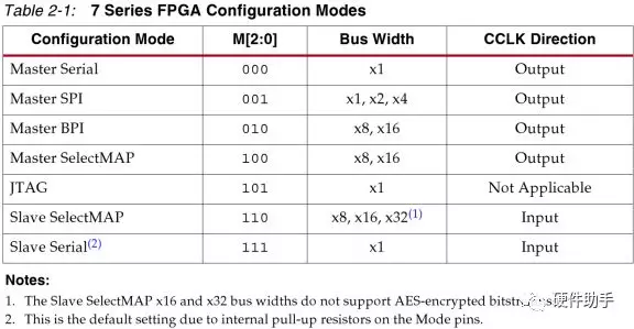
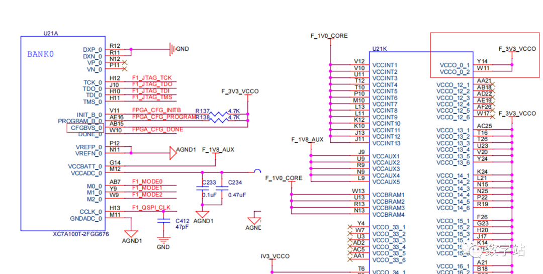
7系列FPGA支持的配置模式如下表所以,每一个系列的bank位置不一样,接口电压也不一样。
每一种模式下对应的引脚定义如下表所示:
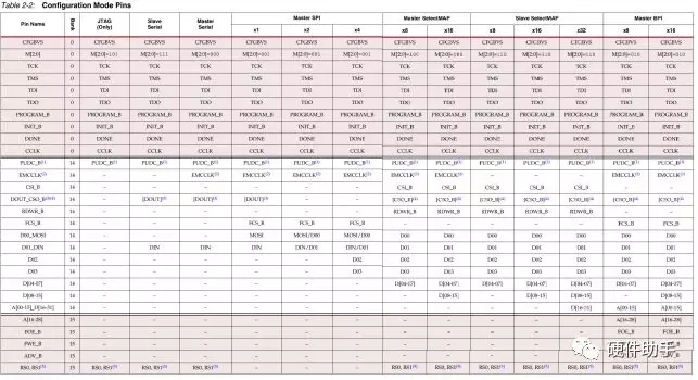
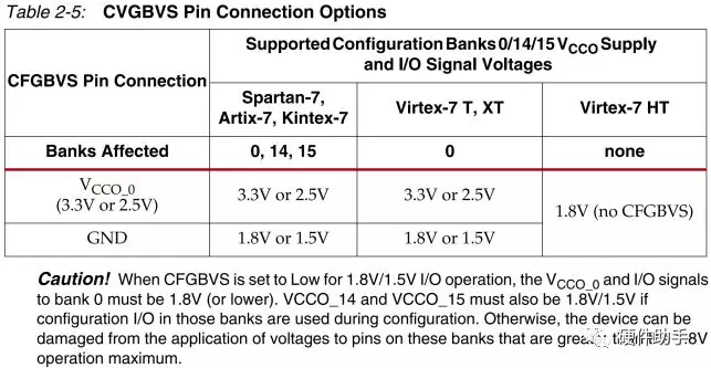
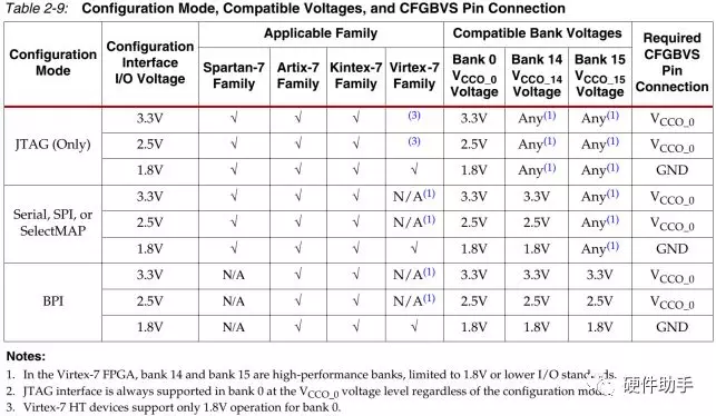
每一个配置引脚的定义此文不再一一罗列,详细参见UG470中的表2-4。其中配置bank的电压选择引脚详细介绍如下:
具体的配置模式较多,每一种都有连接示意图,详细可参见UG470的图2-2(Slave Serial Mode)、图2-5(Single Slave Device SelectMAP Mode)、图2-12(Master SPI x1/x2 Mode)、图2-14(Master SPI x4 Mode)、图2-17(Master BPI Mode-Asynchronous)、图2-20(Master BPI Mode-Synchronous)。另外Master Serial Mode和Slave Serial Mode一样,只是CCLK由FPGA产生。
2、UltraScale系列配置
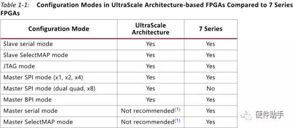
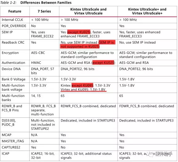
UltraScale系列FPGA的配置和7系列的类似,主要区别如下表所示:
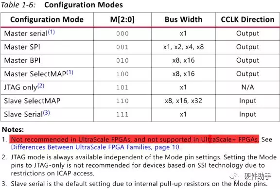
其支持的配置模式如下表所示:
每一种模式下对应的引脚定义如下表所示:

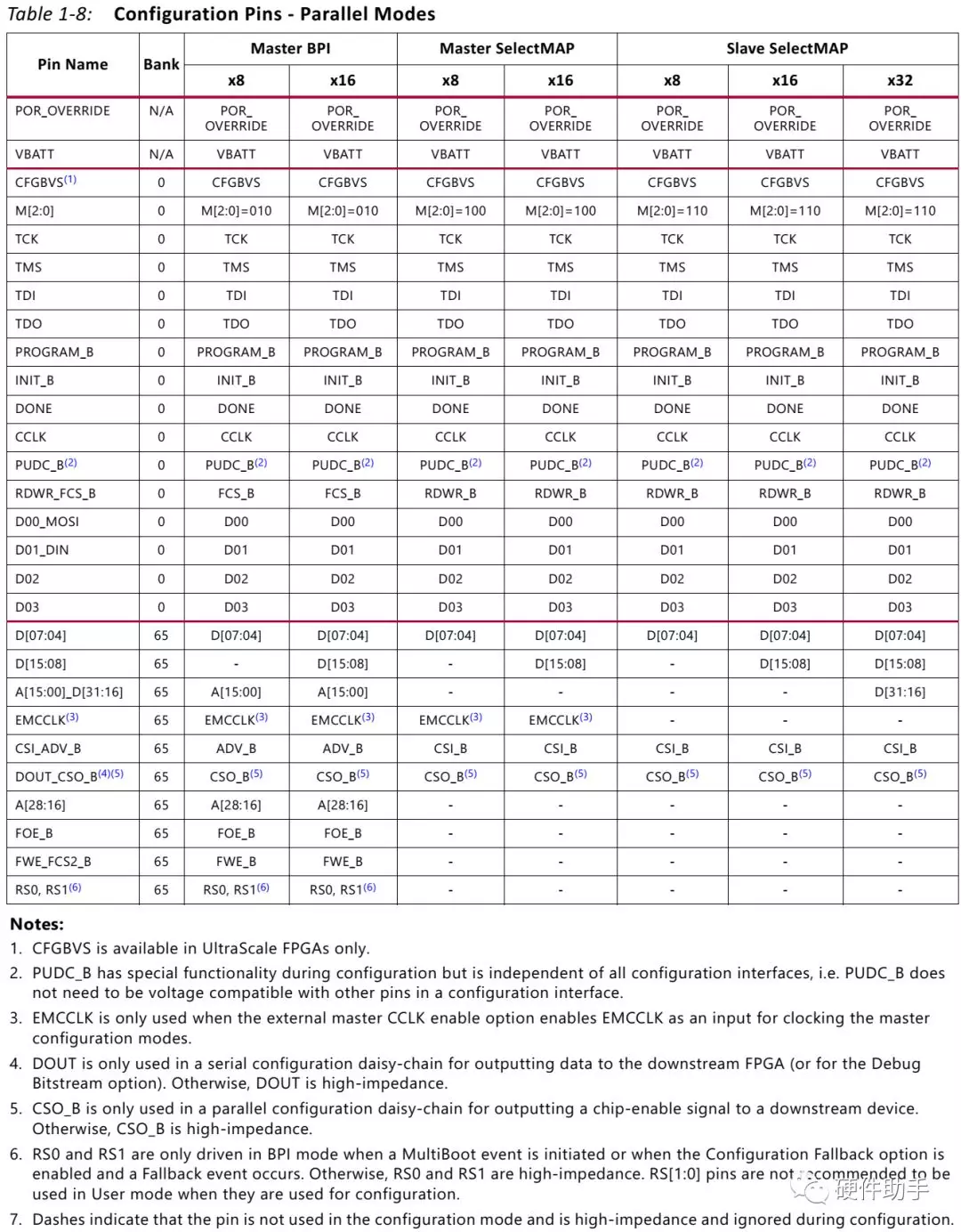
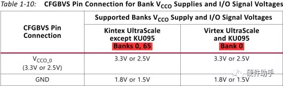
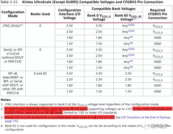
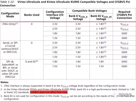
每一个配置引脚的定义此文不再一一罗列,详细参见UG570中的表1-9。其中配置bank的电压选择引脚详细介绍如下:
具体的配置模式较多,每一种都有连接示意图,详细可参见UG570的图2-2(Master SPI x1/x2 Mode)、图2-4(Master SPI x4 Mode)、图2-5(Master SPI x8 Mode)、图3-2(Slave Serial Mode)、图4-2(Master BPI Mode-x16 Synchronous)、图4-4(Master BPI Mode-x16 Synchronous)、图5-2(Slave SelectMAP Mode)。
3、UltraScale+系列配置
UltraScale+系列基本的配置和UltraScale系列一样,主要有以下差异:
Master serial and master SelectMAP configuration modes are not supported in the UltraScale+ FPGAs. These modes are not recommended in the other UltraScale families. (US+不支持Master Serial and Master SelectMAP两种模式。)
The configuration interface can operate only at 1.8V or 1.5V in the UltraScale+ FPGAs. There is no CFGBVS pin in UltraScale+ devices. When migrating from an UltraScale FPGA to an UltraScale+ FPGA, the CFGBVS pin location becomes RSVDGND and must be connected to GND. (US+的配置接口只支持1.8V和1.5V两种电压,没有CFGBVS引脚了,而是预留RSVDGND引脚,如果要使US+系列兼容之前US系列,则该引脚必须接地。)
There is no CFGBVS pin in the Kintex UltraScale+ and Virtex UltraScale+ FPGAs because their configuration I/O only support operation at 1.8V or 1.5V. The pin location is labeled RSVDGND and it must be connected to GND.
The configuration timing and configuration rate options are different between UltraScale FPGAs and UltraScale+ FPGAs. The configuration frame size is 93 32-bit words in the UltraScale+ FPGAs and 123 32-bit words in the UltraScale FPGAs. (配置比特流的大小不一样。)
Bank 65 is an HR bank in most Kintex UltraScale FPGAs(except KU095), an HP bank in the KU095 and Virtex UltraScale FPGAs, and an HP bank in all Kintex UltraScale+ and Virtex UltraScale+ FPGAs.
4、Z7系列配置
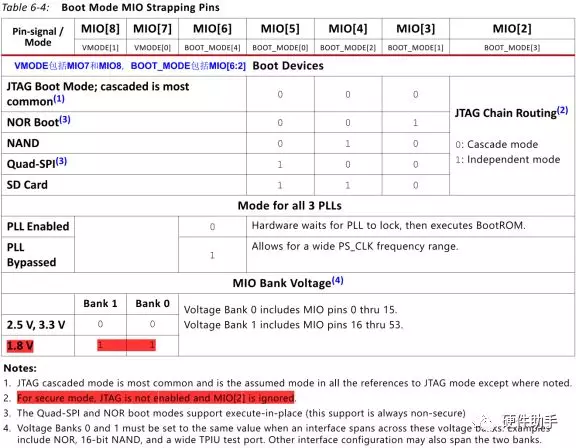
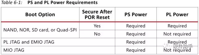
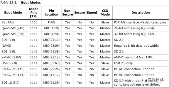
Zynq 7000系列SoC的配置部分全部在ARM侧,除了JTAG从FPGA侧引出之外(虽然对外引出FPGA侧JTAG,但可以将PS部分配置成Cascade模式,这样PL侧和PS侧形成JTAG链),所以其配置遵循ARM处理器的配置,具体支持的模式如下表所示:
对应每一个外设接口的引脚定义如下表所示:
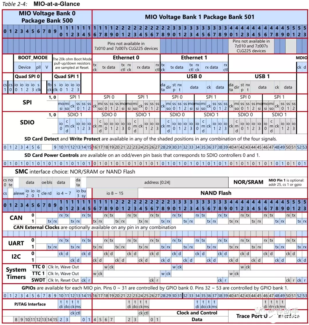
配置相关引脚的处理如下:
MIO[8:2] is used to configure the boot mode, PLL bypass, and MIO voltage. All designs must include a 20 KΩ pull-up or pull-down resistor on these pins to set the required setting.(配置引脚外部使用20K电阻进行上下拉处理)
MIO[8] is a dual use pin that is shared with the high-speed QSPI/NAND/SRAM interface signals. Special care needs to be taken to avoid signal integrity issues. To avoid signal integrity issues, limit the stub length to the pull-up or pull-down resistor to
When system design requires the modes to be changeable, it is recommended to not use a resistor tree to set the mode but instead connect one pull-up/down resistor to the mode pin and place a jumper on the other side of the resistor to select between pull-up or pull-down.(为了便于切换启动模式,可以采用上下拉的方式预留,其实也可以采用拨码开关实现)
The PL system JTAG interface, PL_JTAG, should have its signals TDI, TMS, and TCK pulled-up.(实际芯片内部有上拉)
下面就针对SPI、NAND、NOR、SD Card、JTAG方式进行详细介绍如下:
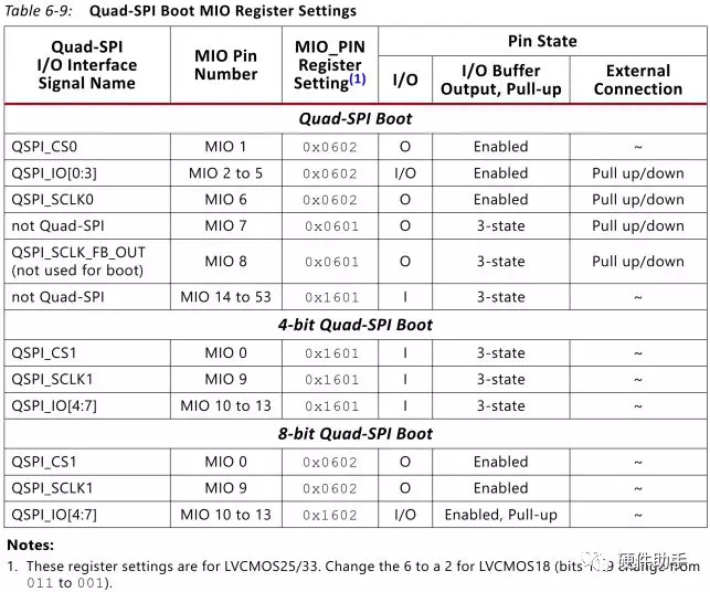
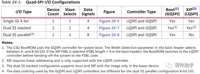
4.1、Quad-SPI Boot
Quad-SPI boot has these features:
x1, x2, and x4 single device configuration.
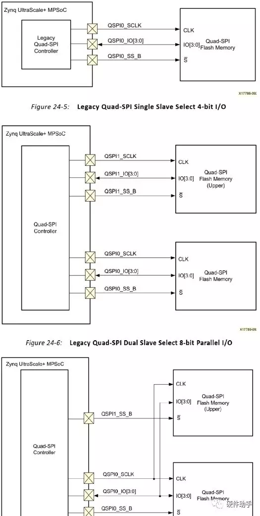
Dual SS, 8-bit parallel I/O device configuration.
Dual SS, 4-bit stacked I/O configuration.
Execute-in-place option.
当使用Quad-SPI模式配置时,如果SPI Flash器件使用的是24bit寻址,则最大只能识别16MB的SPI Flash,如果要使用大于16MB的SPI Flash,则必须支持32bit寻址!!!
SPI boot具体注意事项如下:
The dual SS, 4-bit stacked I/O device configuration is supported, but the BootROM only searches within the first 16 MB address range. The BootROM accesses the device connected to the QSPI0_SS_B slave select signal.
In cases of Quad-SPI boot, if the image is authenticated, then the boot image should be placed at a 32K offset other than 0x0 (the image should not be placed starting at 0x0 offset in Quad-SPI).
There are special reset requirements when using more than 16 MBs of Flash memory. For hardware, refer to AR# 57744 for information. For software considerations, refer to UG821, Zynq-7000 All Programmable SoC Software Developers Guide.
Boot Image requirements when using larger than 16MB QSPI and RSA Authentication (refer AR# 57900).
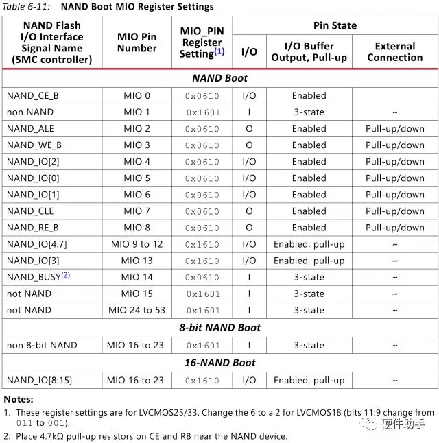
4.2、NAND Boot
NAND boot has these features:
8-bit or 16-bit NAND flash devices
Supports ONFI 1.0 device protocol
Bad block support
1-bit hardware ECC support
使用中的注意事项如下:
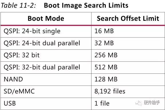
The boot image must be located within the first 128 MB address space of the NAND flash device for the BootROM Header search function.
The BootROM reads the ONFI compliant parameter information in 8-bit mode to determine the device width. If the device is 16 bits wide, then the BootROM enables the upper eight I/O signals for a 16-bit data bus. The 16-bit NAND interface is not available in 7z010 dual core and 7z007s single core CLG225 devices.
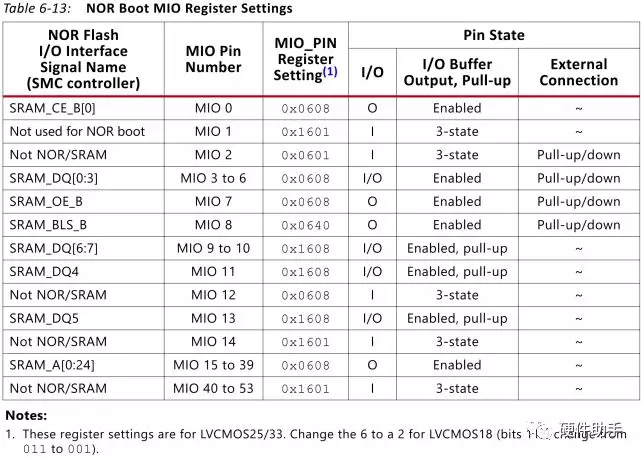
4.3、NOR Boot
NOR boot has these features:
x8 asynchronous flash devices
Densities up to 256 Mb
Execute-in-place option
使用中的注意事项如下:
The BootROM does not try to perform any configuration detection of NOR flash devices. When NOR is the selected boot device, the BootROM programs the MIO pins as shown in Table 6-13.
The NOR interface is not available in 7z010 dual core and 7z007s single core CLG225 devices.
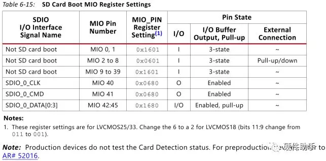
4.4、SD Card Boot
SD card boot supports these features:
Boot from standard SD or SDHC cards
FAT 16/32 file system
Up to 32 GB card densities
使用中的注意事项如下:
The SD card boot mode is not supported in 7z010 dual core and 7z007s single core CLG225 devices.
The SD card boot mode does not support header search or multiboot.
4.5、JTAG
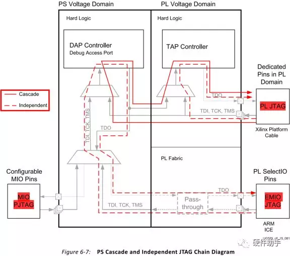
JTAG部分,对外引出的是PL侧的JTAG,但是PS侧的JTAG可以通过Cascade模式从PL侧引出,也可以通过Independent模式从MIO/EMIO引出。
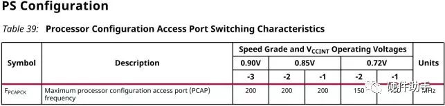
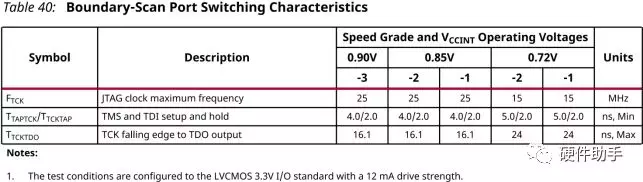
配置时钟的频率是有要求的,不同的电压等级配置时钟频率上限不一样。
Boot Mode引脚的处理如下:
Connect the boot mode pins to a 4.7 kΩ or lower pull-up resister to VCCO_PSIO[3] or pull-down to ground depending on the desired setting.
If multiple switchable boot modes are desired, connect one pull-up/down resistor to the mode pin and place a jumper on the other side of the resistor to select between pull-up or pull-down.
An easily switchable boot mode configuration is recommended for debug ease-of-use.
PS_INIT_B, PS_PROG_B, and PS_DONE引脚处理如下:
Connect PS_INIT_B to a 4.7 kΩ pull-up resistor to VCCO_PSIO[3]. PS_INIT_B is open drain and should not be driven during logic built-in self test (LBIST).
Connect PS_PROG_B to a 4.7 kΩ pull-up resistor to VCCO_PSIO[3]. PS_PROG_B is open drain and should not be driven during LBIST.
Connect PS_DONE to a 4.7 kΩ pull-up resistor to VCCO_PSIO[3].
外部配置支持SPI、NAND、SD、eMMC、USB、JTAG等方式启动,具体如下:
Quad-SPI (24b/32b): The BootROM code can boot Quad-SPI using 24- or 32-bit addressing.
Image search for multi-boot is supported in this boot mode. The QSPI boot mode also supports x1, x2 and x4 read modes for single Quad-SPI memory and x8 for a dual QSPI. This is the only boot mode that supports execute-in-place (XIP).
NAND: The NAND boot mode only supports 8-bit widths for reading the boot images. Image search for multi-boot is supported. Boot mode image search limits are 128MB.
SD0/SD1: These boot modes support FAT 16/32 file systems for reading the boot images. Image search for multi-boot is supported. The maximum number of files that can be searched as part of an image search for multi-boot are 8,192. The SD supported version is 2.0. It only supports 3.3V for the I/Os and up to 4 bits of data interface.
SD1(LS): The SD1-LS boot mode is the same as SD0/SD1 with additional support of the SD 3.0 (with an SD 3.0 compliant voltage level shifter).
eMMC(18): This boot mode is the same as the SD boot mode except it only supports 1.8V for the I/Os and up to 8 bits of data interface.
For SD and eMMC boot modes, the boot image file should be at the root of first partition of the SD card (not inside any directory).
USB0: The USB boot mode configures USB controller 0 into device mode and uses the DFU protocol to communicate with an attached host.
The USB host contains the FSBL boot image (e.g., boot.bin) that is loaded into OCM memory for the CSU BootROM code and an all encompassing boot image file (e.g., boota53_all.bin) that is loaded into DDR memory.
The size of these files are limited by the size of the OCM and DDR memories. The USB boot mode does not support multi-boot, image fallback, or XIP.
每种启动模式的Boot image search limits如下表所示:
针对SPI配置,当使用Quad-SPI模式配置时,如果SPI Flash器件使用的是24bit寻址,则最大只能识别16MB的SPI Flash,如果要使用大于16MB的SPI Flash,则必须使用32bit寻址。如果要使用32bit地址,则SPI Flash的复位必须和FPGA的复位相连,以保证FPGA重新配置时,SPI Flash也能重新配置。
采用SPI Flash进行配置时,由于不同的SPI Flash芯片支持的最大配置时钟频率不一样,一定得同时满足ZU+和SPI Flash两边的时钟限制。
JTAG的配置时钟也是有限制的,根据不同速度等级不一样!详见下表。Place 4.7 kΩ pull-up resistors on the TMS, TCK, and TDI lines.
以上就是针对7 Series、UltraScale、UltraScale+、Zynq 7000、Zynq UltraScale+系列的配置介绍,详细可参见《UG470》、《UG570》、《UG585》、《UG1085》等文档中关于配置的介绍。
编辑:hfy
-
FPGA
+关注
关注
1664文章
22504浏览量
639291 -
Xilinx
+关注
关注
73文章
2208浏览量
131908 -
JTAG
+关注
关注
6文章
415浏览量
75281 -
UltraScale
+关注
关注
0文章
126浏览量
32411
发布评论请先 登录
使用I2C 作为监听模式如何实现
Xilinx FPGA中的混合模式时钟管理器MMCME2_ADV详解


PLL控制器和分辨率模式切换详解

CW32 UART低功耗模式详解
【NCS随笔】如何进入system_off深度睡眠模式以及配置GPIO中断唤醒
一文详解xilinx 7系列FPGA配置技巧
cyw20719B2 SPI接口slave模式下,在执行wiced_hal_pspi_slave_rx_data()函数的同时,SPI的FIFO还能正确接收数据吗?
请问Cyw20791B2 的spi接口在slave模式下最高clk频率是多高?
AMD FPGA异步模式与同步模式的对比
如何配置双模式下的 BT 芯片?
是否可以通过SLAVE FIFO模式或GPIF将2个MPEG-TS解调器连接到FX2LP?
HarmonyOS应用深色模式适配方案


评论