 赛普拉斯低成本高可靠嵌入式闪存技术

Outline
1. Charge-trap eNVMs at Cypress
2. SONOS
–Introduction
–Key Macro Specs
–High Reliability
3. eCT
–Introduction
–Key Macro Specs
–High Reliability
4. Embedded NVM Solutions for Various Applications
Charge-trap eNVMs at Cypress
Cypress develops, uses and licenses two embedded NVM technologies
-
SONOS and eCT,both are charge-trap non-volatile memories.
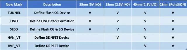
SONOS: Silicon Oxide Nitride Oxide Silicon
-
Originally developed at Sandia National Lab, CY acquired it in 1998.
-
Available at 0.35µm, 0.13µm, 95nm, 65nm, 55nm, 40nm and 28nm process nodes.
-
Shipped>1,200,000 wafers from foundry partners HHGrace, HLMC and UMC.
-
Low cost, Lowpower, suitable for IoT, consumer, industrial, and automotive grade2/3 applications.
eCT : embedded Charge Trap
-
Former Spansion’s eNVM technology for automotive MCUs.
-
Based on 6 generations of Mirror Bit technologies.
-
In production (MCUs) at 40 nm node at UMC.
-
Automotive Grade-1 qualified.
Key Features
SONOS Introduction
Silicon Oxide Nitride Oxide Silicon
-
A planar, scalable MOS transistor with an ONO stack as the gate dielectric.
-
Store captured charges in discrete traps in the nitride (N) layer through FN tunneling.
Low Cost, Low Power, High Security
-
Lowest cost: Only 3~5 extra masks added into standard CMOS process.
-
Lowest power: 7.5V program/erase voltage, low-current FN/FN program/erase operations.
-
High Security: Resistant to decode by de-processing.
-
Ideal solution for consumer, industrial and especially IoT SoCs.
> MCU, Smart Card,EEPROM, FPGA, NOR Flash, etc.
Key SONOS Macro Specs
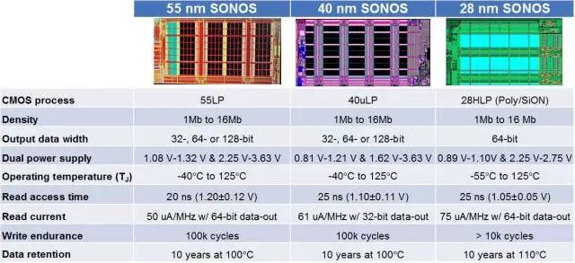
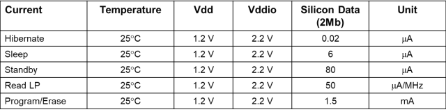
55 nm SONOS Macro Power Consumption
-
Balanced power consumption and performance (20ns Taa) for many applications
−Three power-saving modes: hibernate, sleep and standby.
−Low power read and program/erase operations to minimize active power.
−Low power read operation with Vdd=1.08 V to1.32 V.
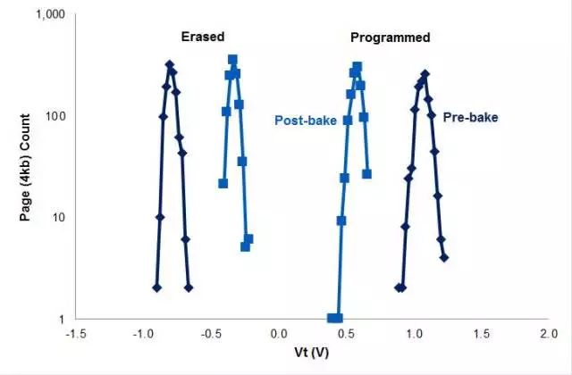
500hrs 225°C Yield w/ 50K Pre-cycling at 85 °C (55nm)
*All dies pass reading on full 8Mb after 500hrs 225°C bake
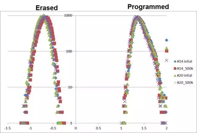
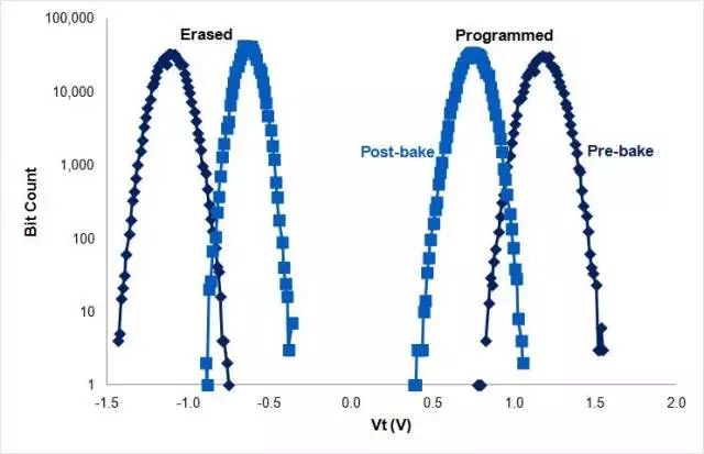
High Reliability
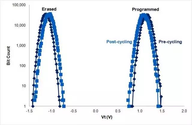
55-nm SONOS Macro Reliability
-
Endurance passes 500K cycles at 85°C w/o ECC. Vt window > 1.2V after 500K cycling.
-
Retention passes Automotive Grade-2 AEC Q100 requirement.
> Vt window > 0.6 V after 500 hrs bake @ 225C with 50K pre-cycling.
>滑动查看下一张图片<
40-nm SONOS Macro Reliability
-
Endurance passes 500K cycles at 85°C w/o ECC. Vt window > 1.2V after 500K cycling.
-
Retention passes Automotive Grade-2 AEC Q100 requirement
>Vt window > 0.6 V after 500 hrs bake @ 225C with 50K pre-cycling.
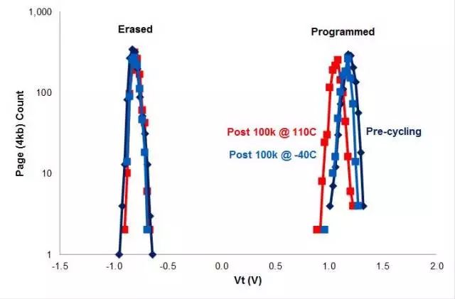
>滑动查看下一张图片<
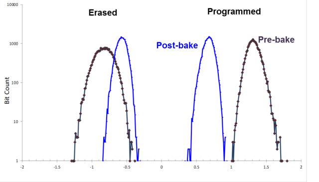
28-nm SONOS Macro Reliability
-
Endurance passes 10K cycles at 125°C, Vt window >1.4 V after cycling.
-
Retention passes accelerated 48-hour bake at 250°C with > 0.7 V window left.
>滑动查看下一张图片<
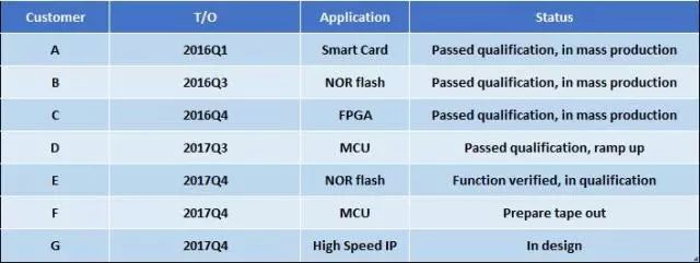
55nm SONOS in Production Press Release
Customers NPI Status @ HLMC 55nm SONOS
-
Engaged > 15 customers.
-
7 Customers signed contract to use
-
3 in mass production
-
> 1,000 wafers started per month
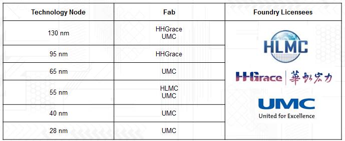
SONOS eNVM Technology Availability
SONOS eNVM is scalable and proven in volume production on many nodes.
eCT Introduction
embedded Charge Trap
-
Based on charge-trap technology proven in six generations of MirrorBit® NOR Flash memory
Ideal solution for high-performance automotive MCUs
-
Fast 8 ns random access time from -40°C to 150°C junction temperature and 30 ms word programming speed
-
Smallest eNVM bit cell in the industry, 0.053 sq. µm, at 40 nm node
-
Automotive Grade-1 reliability
Applications
-
Hybrid and electric vehicle motor control, instrument clusters, body control modules and HVAC
-
In volume production on UMC 40LP process flow
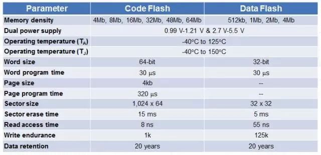
Key eCT Macro Specs
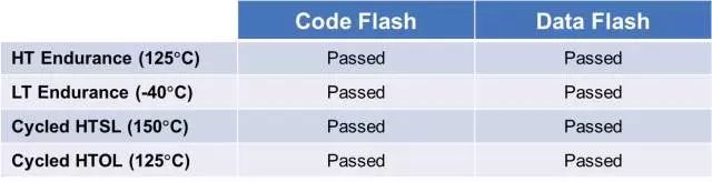
eCTReliability:
Automotive Qualification Data
-
Passed accelerated stress tests for Automotive Grade-1 per AEC-Q100 standard
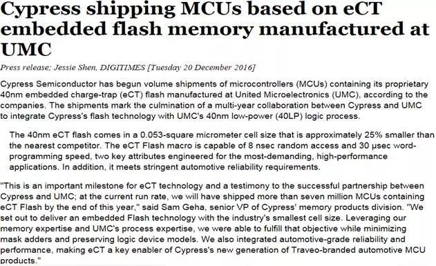
40nm eCT in Production Press Release
Embedded NVM Solutions for Various Applications
Conclusion
Cypress develops and licenses charge-trap NVM technologies and Flash macro IP
-
Charge-trap NVMs serve in a wide range ofembedded applications
−SONOS: Consumer, Industrial SoCs
−eCT: high-performance automotive MCUs,Automotive Grade-1 reliability
-
Technologies are scalable to advanced nodes
−SONOS in mass production from 0.35um to 55nm, engineering samples available on 40uLP & 28HLP
−eCT is in volume production on UMC 40LP process
-
Low power for IoT: 0.9 V (40nm) or 1.2V(55nm) power supply, low-current operation, power-saving modes
-
Cost-effective: 3~5 (SONOS) or 8 (eCT)extra masks beyond the standard CMOS.
-
赛普拉斯
+关注
关注
28文章
395浏览量
89033 -
低功耗
+关注
关注
12文章
4120浏览量
106937
原文标题:赛普拉斯低成本高可靠嵌入式闪存技术
文章出处:【微信号:CypressChina,微信公众号:Cypress教程】欢迎添加关注!文章转载请注明出处。
发布评论请先 登录
RoboPeak Mini USB Display:低成本嵌入式显示模块的理想之选

S6E1C系列32位ARM® Cortex®-M0+ FM0+微控制器深度解析
铠侠UFS 5.0嵌入式闪存出样
【正式来袭】2026年嵌赛——瑞芯微 飞凌嵌入式赛题解读

什么是嵌入式应用开发?
arm嵌入式主板优缺点
系统嵌入式的学习路线
探索Series 660低成本可嵌入式加速度计:应用与技术解析
Cypress赛普拉斯FRAM增强车载黑匣子EDR抗干扰能力

嵌入式和FPGA的区别
2025全国大学生嵌入式芯片与系统设计竞赛应用赛道全国总决赛圆满闭幕-飞凌嵌入式

【技术指南】提升嵌入式数据可靠性,从元器件选型开始!

赛普拉斯FRAM宽温域生命守护


评论