 如何为MSP430设计固件以收集和处理IC的数据

入门
如今,无需进行一些编程就很难创建任何电子电路。不幸的是,您学习为一个制造商创建固件的知识不一定适用于另一个制造商。
出于这个原因,购买评估板通常是一个好主意,这样您就可以学习在一个肯定可以正常工作的板上对您的微控制器进行编程,然后再用自己的设计来解决问题。熟悉制造商为您提供的资源(论坛、数据表、用户指南、视频等)也是一个好主意。
在这种情况下,我使用了MSP430FR2633,因此我在MSP CapTIvate MCU 开发套件上进行了练习,并向TI 的 E2E 社区寻求建议。
本文并未涵盖源代码的每一行;相反,它以源代码为例提供了有关固件编程的一般信息。
添加 ASCII 引脚图
最后,我想为自己添加一些额外的参考。由于这是一个自定义板,我想在一个位置向自己提供尽可能多的信息。很有可能一个小时后我不会记得我的引脚连接是什么,而且我肯定不会记得一个星期后。如果我进行任何编程更改,不必挖掘原理图会很好。
出于这个原因,我在源代码中包含了一个连接图。网络上有各种ASCII 图表生成器,这使得操作相对快速。
//   CP2102N           ┌──────┬──────┐            ┌────────────┐
// ┌────────────┐      │      │ P1.0 │→ UCB0STE  →│ EN (NC)    │
// │    USB     │→ RX →│ P2.5 │ P1.1 │→ UCB0CLK  →│ CLK        │
// │    TO      │→ TX ←│ P2.6 │ P1.2 │→ UCBSIMO  →│ SIMO (NC)  │
// │   UART     │      │      │ P1.3 │← UCBSOMI  ←│ SOMI       │
// └────────────┘      ├──────┼──────┤            │            │
//             ST_IN1 ←│ P2.0 │ P2.4 │← BUSY     ←│ BUSY       │
//             ST_IN2 →│ P2.1 │ P3.0 │→ RDL      →│ RDL        │
//                     │      │ P3.1 │→ CNV      →│ CNV        │
//                     └──────┴──────┘            └────────────┘
//                       MSP430FR2633                 ADC
我们需要做的第一件事是处理我们的引脚,以便编译器知道哪些设备连接到什么。为此,您需要了解寄存器的概念。如果您已经熟悉这些概念,请随意跳到下面的“定义寄存器描述快捷方式”。
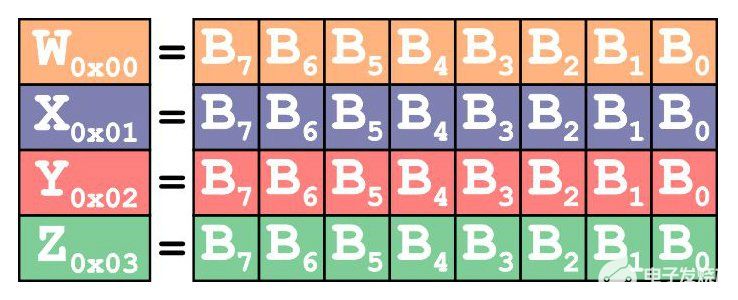
什么是寄存器?
寄存器是内存中由十六进制数字标识的位置,位属于寄存器。每个寄存器中的位控制微控制器功能的特定方面。
每个寄存器控制一个字节(8 位)或一个字(16 位)。然而,为了使讨论简单,下图说明了控制单个字节的寄存器。
定义寄存器描述快捷方式
现在我们对寄存器有了非常简短的背景,让我们在上下文中使用它。
MSP430FR2xx 系列用户指南中的寄存器描述指示哪些位控制哪些功能。当寄存器不允许直接访问单个位时,您可以将字节操作与适当的位掩码结合使用;单个位可以使用“|=”运算符设置,使用“&=”运算符清除,或使用“^=”运算符切换。
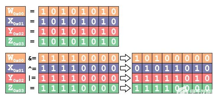
上图显示了四种字节操作前后虚寄存器 W、X、Y 和 Z 中的数据。
配置位在数据表中以十六进制或二进制表示法提供。但是,键入诸如 0x3F2A &= 0xC9 之类的内容并跟踪程序中发生的事情是相当不方便的。因此寄存器和引脚名称在引用的头文件中或在程序的开头定义。并且使用寄存器的名称和与该寄存器关联的引脚而不是原始的十六进制和二进制数。例如,“WDTCTL = WDTHOLD”(WatchDog Timer ConTroL 寄存器 = WatchDog Timer HOLD 值)—换句话说,停止看门狗定时器。
因此,编程不再使用十六进制地址,而是使用这些命名的快捷方式指定寄存器和位,并直接或使用字节操作(例如上面提到的那些)修改位。
void main(void)
{
    WDTCTL = (WDTPW | WDTHOLD);         // Stop watchdog timer
    …
    CSCTL3 |= SELREF__REFOCLK;          // Set REFO as FLL reference source
    CSCTL0 = 0;                         // clear DCO and MOD registers
    CSCTL1 &= ~(DCORSEL_7);             // Clear DCO frequency select bits first
    CSCTL1 |= DCORSEL_5;                // Set DCO = 16MHz
    …
命名变量——引脚的位位置
对于 MSP430,每个端口控制一组引脚 — GPIO 通常为 8 位,因此一个端口对应一个字节。虽然您不能立即定义端口,但控制端口引脚的寄存器不可位寻址,因此无法创建与单个引脚对应的名称(例如,“#define somePinVar 1.5”)。
相反,我们将名称附加到引脚的位位置,并使用该名称与端口寄存器一起控制它。
首先命名引脚(它们所连接的端口将在程序后面说明)。这可以在主程序的开头或在单独的头文件中完成。选择变量和常量的名称是为了便于以后理解,并基于 PCB 上相应的网络名称。
#define UART_RX_PIN     BIT5            // P2.5 eUSCI_A1
#define UART_TX_PIN     BIT6            // P2.6 eUSCI_A1

#define SPI_EN_PIN      BIT0            // P1.0 eUSCI_B0 -- not used
#define SPI_CLK_PIN     BIT1            // P1.1 eUSCI_B0
#define SPI_MOSI_PIN    BIT2            // P1.2 eUSCI_B0 -- not used yet
#define SPI_MISO_PIN    BIT3            // P1.3 eUSCI_B0

#define ADC24_RDL       BIT0            // P3.0 set low always
#define ADC24_CNV       BIT1            // P3.1 L->H->L (20 ns) to convert
#define ADC24_BUSY      BIT4            // P2.4 goes low after conversion

#define ST_IN1          BIT0            // 3PST switch input 0
#define ST_IN2          BIT1            // 3PST switch input 1
程序的下一部分定义了使用的变量以及函数原型。我使用全局变量并将数组保留为易失性,以避免 SPI 和 UART 中断服务例程的任何潜在问题。本节中定义的所有变量都可用于所有函数。
// Variable Declarations
…
uint16_t numTrials;                     // number of times to repeat reads
uint16_t numReads;                      // number of conversions per read
…
uint8_t byteCounter;                    // need 24 bits + 16 bits (5 bytes)
volatile uint8_t dataBuffer[5];         // Holder for all SPI data

// Function Prototypes
void readADC(uint16_t);                 // Runs conversions
uint8_t spix(uint8_t);                  // SPI interface communication
void uartx(uint8_t);                    // UART interface communication one-way
分配引脚功能
MSP430FR2633 具有可支持多种功能的引脚。因此,必须告知 MCU 引脚是用于通用输入/输出还是用于UART或I 2 C等集成外设。
以下几行代码配置端口 2 使用,首先为 UART Tx/Rx 连接对应的端口 2 引脚选择备用功能(即集成外设),然后配置 UART_TX 引脚和两个自检开关引脚作为输出。
    // Select module function for UART (page 63)
    P2SEL0 |= (UART_TX_PIN | UART_RX_PIN);
    // Set port pins as output for UART and SP3T Switch
    P2DIR |= (UART_TX_PIN | ST_IN1 | ST_IN2);
自定义函数
自定义函数用于读取 ADC — 基本上只是切换启动转换标志,等待繁忙指示器关闭,然后再次切换启动转换标志 — 由在开始时设置的常数所指示的次数该程序。
void readADC(uint16_t numReads)
{
// Start conversion, wait for busy flag to turn off,
// and start the next conversion.
    for (counter = 1; counter <= numReads; counter++)
    {
        P3OUT ^= ADC24_CNV;     // Toggle convert flag high > 20 ns to start
        __delay_cycles(1);      // measurement.  1/16MHz * 1 cycles = 62.5 ns
        P3OUT &= ~ADC24_CNV;    // Set convert flag back low
// Wait to let conversion finish - might never enter function
        while ((P2IN & ADC24_BUSY))
        {
            __delay_cycles(1);     // 1/16Mhz = 62.5 ns
        }
    }
收集数据
数据将从我的微控制器中出来,并通过 USB 快速传输到 PC。如果我在通过 UART 到 USB 转换器发送数据之前将此数据转换为十进制等效值或度/分/秒,则很难看到数据以每秒约 100 行的速度滚动时有多稳定。相反,我们将数据转换为二进制。
通过将数据转换为二进制,我可以在串行监视器中快速查看有多少未更改的位,只需从左侧开始计数。一旦位开始变化,我就会遇到噪音(当然,假设传感器完全静止)。数据以我在完整程序中用制表符分隔的块的形式出现:三个字节用于角度数据,两个字节用于每次读取的样本数(我后来又添加了两个字节来创建一个计数器)。
    for (byteCounter = 0; byteCounter < 5; byteCounter++) //0,1,2,3,4
    { for (bitCounter = 0; bitCounter < 8; bitCounter++)
        { if (((dataBuffer[byteCounter] >> (7 - bitCounter)) & 0b1) == 0)
            { uartx('0'); // ASCII 0 }
            Else { uartx('1'); // Ascii 1 }
        }
您会注意到我必须更改每个字节的“字节顺序”,以便它首先到达 UART MSB。
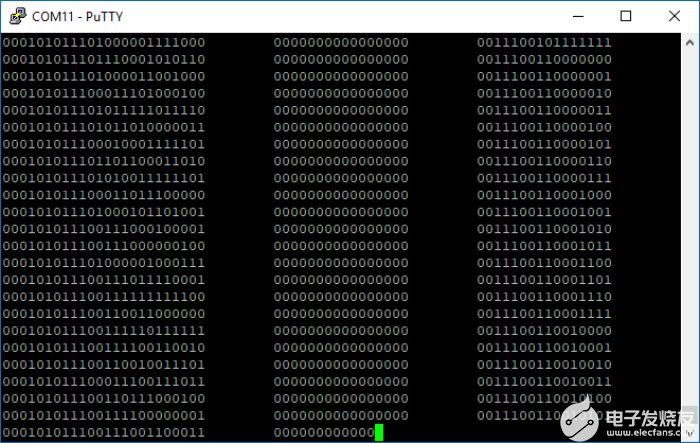
样本数据显示了 ADC 读数的一列、自上次数据传输以来读取的读数数量以及一个计数器。
使用 Mathematica 处理数据
在最终程序中,我最终添加了一个试用计数器并使用Mathematica(在Rasbian OS上免费)处理数据。未来的文章将更详细地解释数据和数据处理。
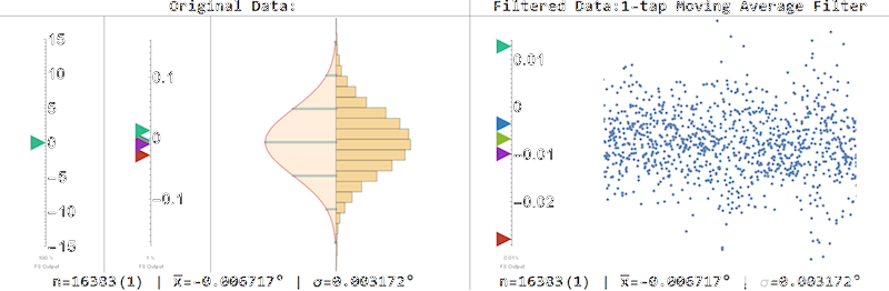
初步试验的数据如上所示。带有彩色三角形的垂直刻度显示三个缩放级别的最大值、+1σ、平均值、-1σ 和最小值。还包括散点图、直方图及其伴随的理想化正态分布。
本文解释了该项目的一小部分固件编程。下一篇文章将描述设备中的噪声,未来的文章将分析数据。
您将在下面找到 MCU 上程序的完整源代码的可下载文件。如果您也有兴趣访问 Mathematica 源代码文件,请在下面的评论中告诉我!
Precision_Inclinometer_Firmware.zip
//         _ _          _                 _    _____ _                _ _
//   /\   | | |   /\   | |               | |  / ____(_)              (_) |
//  /  \  | | |  /  \  | |__   ___  _   _| |_| |     _ _ __ ___ _   _ _| |_ ___
// / /\ \ | | | / /\ \ | '_ \ / _ \| | | | __| |    | | '__/ __| | | | | __/ __|
/// ____ \| | |/ ____ \| |_) | (_) | |_| | |_| |____| | | | (__| |_| | | |_\__ \
//_/    \_\_|_/_/    \_\_.__/ \___/ \__,_|\__|\_____|_|_|  \___|\__,_|_|\__|___/
//                      _____         _         __    _____         _
//                     |     |___ ___| |_    __|  |  |  |  |_ _ ___| |_ ___ ___
//                     | | | | .'|  _| '_|  |  |  |  |     | | | . |   | -_|_ -|
//                     |_|_|_|__,|_| |_,_|  |_____|  |__|__|___|_  |_|_|___|___|
//                     w/ support by Bruce McKenney            |___|  2018/11/09
//            _ __
//           ' )  )   _/_
//  ______ . ./--'__. / __.
// / / / <(_//  \(_/|<_(_/|_
//  __ __ _  ___ __   __ __ _  __  _  _ ____ ____ ____ ____
// (  |  ( \/ __|  ) (  |  ( \/  \( \/ |  __|_  _|  __|  _ \
//  )(/    ( (__/ (_/\)(/    (  O ) \/ \) _)  )(  ) _) )   /
// (__)_)__)\___)____(__)_)__)\__/\_)(_(____)(__)(____|__\_)
//
/****************************** Connection Diagram ****************************/
//   CP2102N           ┌──────┬──────┐            ┌────────────┐
// ┌────────────┐      │      │ P1.0 │→ UCB0STE  →│ EN (NC)    │
// │    USB     │→ RX →│ P2.5 │ P1.1 │→ UCB0CLK  →│ CLK        │
// │    TO      │→ TX ←│ P2.6 │ P1.2 │→ UCBSIMO  →│ SIMO (NC)  │
// │   UART     │      │      │ P1.3 │← UCBSOMI  ←│ SOMI       │
// └────────────┘      ├──────┼──────┤            │            │
//             ST_IN1 ←│ P2.0 │ P2.4 │← BUSY     ←│ BUSY       │
//             ST_IN2 →│ P2.1 │ P3.0 │→ RDL      →│ RDL        │
//                     │      │ P3.1 │→ CNV      →│ CNV        │
//                     └──────┴──────┘            └────────────┘
//                       MSP430FR2633                 ADC
/********************************* Description ********************************/
// by Mark Hughes for AllAboutCircuits.com.  Find complete information for this
// project at http://allaboutcircuits.com/author/mark-hughes
// This is a one-directional SPI to UART to USB bridge interface
// CNV is toggled one/multiple times (up to 65535) and data is averaged inside
// the ADC until SPI_CLK toggles data out and into MSP430.  Data is then sent
// via UART to CP2102N at 115200, and then from the CP2102N to the computer.
// The data is sent over UART in Binary format MSB first using ASCII characters.
// self-test and auto-calibration not yet implemented.
// When ST_IN1 != ST_IN2, enters self-test mode for sensor
/*********************************** Headers **********************************/
#include
#include
#include

/******************************* Pin Definitions ******************************/
#define UART_RX_PIN     BIT5            // P2.5 eUSCI_A1
#define UART_TX_PIN     BIT6            // P2.6 eUSCI_A1

#define SPI_EN_PIN      BIT0            // P1.0 eUSCI_B0 -- not used
#define SPI_CLK_PIN     BIT1            // P1.1 eUSCI_B0
#define SPI_MOSI_PIN    BIT2            // P1.2 eUSCI_B0 -- not used yet
#define SPI_MISO_PIN    BIT3            // P1.3 eUSCI_B0

#define ADC24_RDL       BIT0            // P3.0 set low always
#define ADC24_CNV       BIT1            // P3.1 L->H->L (20 ns) to convert
#define ADC24_BUSY      BIT4            // P2.4 goes low after conversion

#define ST_IN1          BIT0            // 3PST switch input 0
#define ST_IN2          BIT1            // 3PST switch input 1

/**************************** Variable Declarations ***************************/
// Can be consolidated and revised later with proper function calls and
// data returns later on.
uint8_t bitCounter;                     // 0-7 counter for bits in a byte.
uint8_t byteCounterSPI;                 // 0-4 counter for SPI data bytes.
uint8_t byteCounter;                    // need 24 bits + 16 bits (5 bytes)
uint16_t counter;                       // Temporary counter
uint16_t numTrials;                     // Temporary counter
uint16_t numTrialsMax = 1024;           // Number of times to repeat measurement
uint16_t numReads = 4;                  // number of conversions per read.

// Can replace volatile buffer with pointer later on.
volatile uint8_t dataBuffer[5];         // Holder for all SPI data

/****************************** Function Prototypes ***************************/
// Function Prototypes
void readADC(uint16_t);                 // Decides number of conversions
uint8_t spix(uint8_t);                  // SPI interface
void uartx(uint8_t);                    // UART interface

/******************************** Main Program ********************************/
void main(void)
{
    //********************* Begin Configuration ********************************

    WDTCTL = (WDTPW | WDTHOLD);         // Stop watchdog timer
    FRCTL0 = FRCTLPW | NWAITS_1;        // FRAM configuration for > 8 MHz
    __bis_SR_register(SCG0);            // Disable Frequency Locked Loop (FLL)
    CSCTL3 |= SELREF__REFOCLK;          // Set REFO as FLL reference source
    CSCTL0 = 0;                         // Clear DCO and MOD registers
    CSCTL1 &= ~(DCORSEL_7);             // Clear DCO frequency select bits first
    CSCTL1 |= DCORSEL_5;                // Set DCO = 16MHz
    CSCTL2 = FLLD_0 + 487;              // DCOCLKDIV = 16MHz
    __delay_cycles(3);                  // Wait to allow stabilization of clock
    __bic_SR_register(SCG0);            // Reenable FLL
    while (CSCTL7 & (FLLUNLOCK0 | FLLUNLOCK1))
        /*EMPTY*/;            // FLL locked
    // default DCOCLKDIV as MCLK and SMCLK source
    CSCTL4 = SELMS__DCOCLKDIV | SELA__REFOCLK;
    // Disable GPIO power-on default high-impedance mode
    PM5CTL0 &= ~LOCKLPM5;   // Disable GPIO power-on default high-impedance mode
    // PxDIR: 0(In) 1(Out)
    // PxSEL: Function Select Register (see datasheet)
    // PxOUT: 0(L) 1(H): Output Register
    // PxREN: 0(L) 1(En): Resistor Enable (on input only)

    // Select SPI module function for SPI (page 60)
    P1SEL0 |= (SPI_MISO_PIN | SPI_MOSI_PIN | SPI_CLK_PIN);
    // Set MOSI and CLK as outputs.
    P1DIR |= (SPI_MOSI_PIN | SPI_CLK_PIN);

    // Select module function for UART (page 63)
    P2SEL0 |= (UART_TX_PIN | UART_RX_PIN);
    // Set port pins for UART and SP3T Switch
    P2DIR |= (UART_TX_PIN | ST_IN1 | ST_IN2);
    // IN1/IN2 initially low to open SPST switch.
    P2OUT &= ~(ST_IN1 | ST_IN2);

    // Set port pins for ADC
    P3SEL0 &= ~(ADC24_RDL | ADC24_CNV);
    // Set direction for RDL and CNV
    P3DIR |= (ADC24_RDL | ADC24_CNV);
    // Set port output low for RDL and CNV
    P3OUT &= ~(ADC24_RDL | ADC24_CNV);

    // Setup SPI in UCB0 Control Word 0
    // Place UCB in reset state before modifying settings

    UCB0CTLW0 |= UCSWRST;
    // Master-mode, synchronous clock, inactive state high, MSB first.
    UCB0CTLW0 |= (UCMST | UCMSB | UCCKPH | UCSYNC | UCMSB | UCSSEL__SMCLK);
    // Bit clock prescaler
    UCB0BRW = 0x0002;   // Bit rate clock = SMCLK/2 = 8 MHz
    // Release reset and initialize state machine
    UCB0CTLW0 &= ~UCSWRST;

    // Put UCA state machine in reset, select mode and clock.
    UCA1CTLW0 = UCMODE_0 | UCSSEL__SMCLK | UCSWRST; // UART, SMCLK, Reset
    // 16M/(UCOS)16/9600 UCA1BRW = 104
    // UCA1BRW = 104;
    // UCBRS=0xD6, 16x oversample, UCBRF=2
    // UCA1MCTLW = (0xD6 << 8) | UCOS16 | UCBRF_2;
    // 16M/(UCOS)16/115200 UCA1BRW = 8;
    UCA1BRW = 8; // 115200 Baud.
    UCA1MCTLW = (0xD6 << 8) | UCOS16 | UCBRF_11;  // 115200 Baud.

    // Release reset and initialize state machine
    UCA1CTLW0 &= ~UCSWRST;

    /**************************** End Configuration ***************************/

    /****************************** Main Program ******************************/
    // Read the ADC a certain number of times.  Toggle ST_IN1 and ST_IN2 to
    // flash LED after certain number of reads.
    for (numTrials = 1; numTrials <= numTrialsMax; numTrials++)
    {
        // Turn LEDS on/off every 100 trials
        if (numTrials % 100 == 1)
        {
            P2OUT ^= (ST_IN1 | ST_IN2);
        }
        __delay_cycles(1);
        readADC(numReads);              // Perform n conversions
    }
    // Turn LEDS off because numTrials likely didn't.
    P2OUT &= ~(ST_IN1 | ST_IN2);

    // Add an additional carriage return and newline.
    uartx('\r'); // Carriage return
    uartx('\n'); // Newline
// End main.
}

/**************************** Function to read ADC ****************************/
void readADC(uint16_t numReads)
{
// Start conversion, wait for busy to turn off, and start the next conversion.
    for (counter = 1; counter <= numReads; counter++)
    {
        P3OUT ^= ADC24_CNV;     // Toggle convert flag high > 20 ns to start
        __delay_cycles(1);      // measurement.  1/16MHz * 1 cycles = 62.5 ns
        P3OUT &= ~ADC24_CNV;    // Set convert flag back low

        // Wait to let conversion finish - might never enter function
        while ((P2IN & ADC24_BUSY))
        {
            __delay_cycles(1);     // 1/16Mhz = 62.5 ns
        }
    }

    // Shift out dummy bytes to allow ADC data to shift into dataBuffer[]
    for (byteCounterSPI = 0; byteCounterSPI < 5; byteCounterSPI++)
    {   // Shift out useless data to allow shift in of ADC data.
        dataBuffer[byteCounterSPI] = spix(0xFF);
    }

    // Find binary equivalent of each dataBuffer byte.  Send it out over UART.
    // Each byte is shifted to the right n-bits and the LSB is read as 1 or 0
    // (7 - bitCounter) is used to change Endianess.
    for (byteCounter = 0; byteCounter < 5; byteCounter++) //0,1,2,3,4
    {
        for (bitCounter = 0; bitCounter < 8; bitCounter++) //0,1,2,3,4,5,6,7
        {
            // Need to change endianness of data before sending out UART
            if (((dataBuffer[byteCounter] >> (7 - bitCounter)) & 0b1) == 0)
            {
                uartx('0'); // ASCII 0
            }
            else
            {
                uartx('1'); // Ascii 1
            }
        }

        // Data Formatting
        if (byteCounter == 2)
        {
            // After the three data-bytes, add a tab to separate number of reads
            uartx('\t'); // Ascii tab
        }

        // After the last byte is out, send a carriage return and line feed.
        if (byteCounter == 4)
        {
            uartx('\t');

            for (bitCounter = 0; bitCounter < 16; bitCounter++)
            {
                if (((numTrials >> (15 - bitCounter)) & 0b1) == 0)
                {
                    uartx('0'); // ASCII 0
                }
                else
                {
                    uartx('1'); // Ascii 1
                }
            }

            uartx('\r'); // Return
            uartx('\n'); // Line Feed
        }
    }
    return;
}

uint8_t spix(uint8_t c)
{
    while (!(UCB0IFG & UCTXIFG))
        /*EMPTY*/;
    UCB0TXBUF = c;
    while (!(UCB0IFG & UCRXIFG))
        /*EMPTY*/;
    c = UCB0RXBUF;
    return (c);
}

void uartx(uint8_t c)
{
    while (!(UCA1IFG & UCTXIFG))
        /*EMPTY*/;
    UCA1TXBUF = c;
    return;

}
-
微控制器
+关注
关注
49文章
8915浏览量
166091 -
msp430
+关注
关注
182文章
2406浏览量
233851 -
开发板
+关注
关注
26文章
6527浏览量
121418
发布评论请先 登录
请问有没有办法对MSP430的固件升级?
FPGA与MSP430系统
MSP430 的Bluetooth连接设计
MSP430简介

MSP430 MCUs, Passive RF and Low-Power RF Solutions Guide能量收集
关于MSP430单片机的USB接口固件编程的研究
MSP430微处理器Value Line介绍
基于MSP430的智能窗户设计方案


评论