

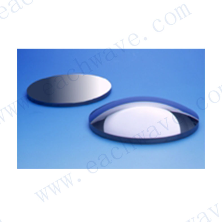
Silicon Elements for IR Objective Lenses
资料下载:Download Silicon Elements for IR Objective Lenses Datasheet (PDF, 144 KB)
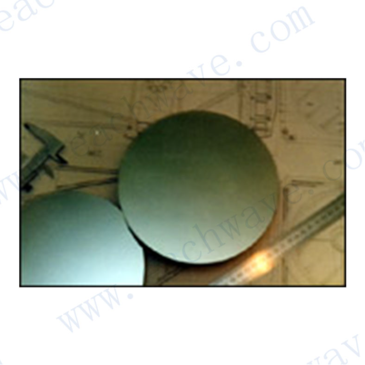
TYDEX produces a wide range of elements made of silicon. We ensure strong control on every step of element production, from material selection to the measurement of obtained parameters of polished elements and coating characteristics. That is especially important in the manufacturing of precision imaging systems. This type of approach to the production of a set of large silicon optics for IR objective is described below.
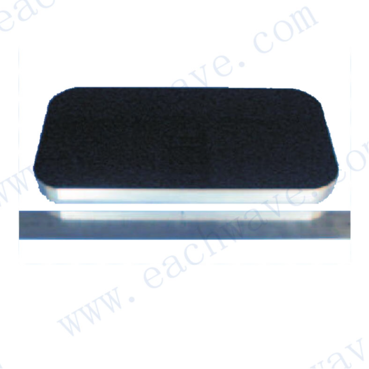
The objective is intended for operating in two middle IR bands: 1.6 - 3.0mm and 3.5 - 5.5 mm. Its design incorporates 17 elements: 14 meniscus and plano-convex lenses with diameters from 10 mm to 210 mm and 3 plates with dimensions to 134 x 198 mm.
When manufacturing such multi-element imaging devices two important points should be taken into consideration: transmittance of the whole system and image distortion. These parameters depend on material quality (i) and surface accuracy (ii). Below we discuss our approach to control of these parameters (we will not touch the third critical point - coating parameters).
Material selection and control
For imaging systems the right choice of material is of utmost very importance. Defects in the material can cause image distortion and violate the system operation. This is the reason why so much attention is paid to selecting the material and its control. To provide the proper quality of material, silicon ingots with special parameters (dislocation-free optical grade monocrystalline Cz-Si with high homogeneity and transparency in the working range) were grown. After a few required ingots with diameter to 219 mm were ready the quality of material (resistance homogeneity, dislocation density, transmittance in the working range) is being controlled on samples prepared from each ingot. The typical transmission curve is presented here.
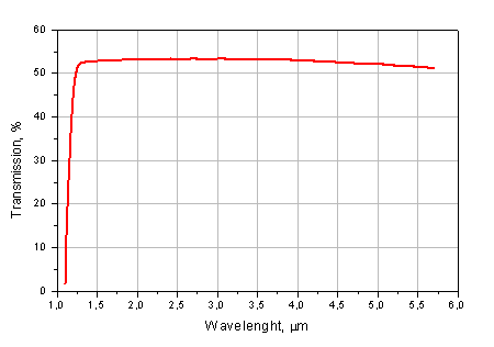
Fig. 1 Silicon transmission in the 1.1 - 5.7 mm spectral range. Sample thikness is 10 mm.
Surface accuracy control
As mentioned above, the second important parameter that should be considered is surface errors. Modern equipment allows to carry out complete interferometric control of a the whole surface or any part of it. Computer data processing enables us to obtain detailed information about different kinds of errors: regular errors (astigmatism, zonal error, coma), local errors, peak-to-valley value etc. In addition, representation of errors becomes easy to interpret.
For interferometric control Fizeau scheme is applied, λc = 632.8 nm (HeNe laser line). Additional equipment such as telescopic expanders and measuring objectives is used if required by surface shape and radius of curvature. Evaluation of the form error of a surface is being carried out in phase mode by means of measuring the deformation of the wavefront reflected from the controlled surface compared to test reference surface. Specialised integrated software is used to create phase data arrays and their further power polynomial approximation for surface error calculations.
Here we present as examples the results of such control for 2 surfaces: 1 - concave surface of meniscus D210 mm lens, and 2 - plane surface of 198 x 134 mm plate.
Interferometric measurements of errors of meniscus lens D210 mm
| concave R = -206.99 clear aperture - central D206 microns sphere |
Regular errors:
| D= .080 | LX= 2.839 | LY= -.013 | C= 2.829 | RMS(W)= .031 | |
| A= .050 | FIA= .354 | RMS(W-A)= .023 | FA= .442 | ||
| B0= -.025 | RZ= .037 | ||||
| RMS(W-Z)= .029 | FZ= .131 | ||||
| B2= .149 | |||||
| B4= -.149 | |||||
| C= .110 | FIC= 164.892 | RMS(W-C)= .028 | FC= .178 | ||
Local errors:
| R= .139 | RMS(M)= .015 |
Parameters of surface:
| RMS | MIN | MAX | R | STRL | STRH |
| .031 | -.144 | .092 | .237 | .964 | .988 |
| X : | -1.000 | .000 |
| Y : | .000 | -1.000 |
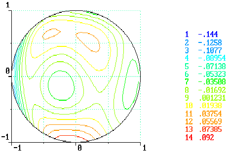
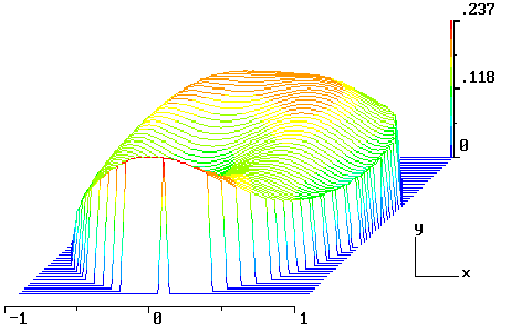
Fig. 2 Reconstracted wavefront topography presented at planar and 3-d plots.
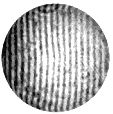
Fig. 3 Interferogram of the surface.
Interferometric measurements of errors of plane parallel plate 198x134 mm
The surface undergoes measurements in 2 areas: center zone of dimensions 70 x 70 mm (approximately the area occupied by incident ray) and the whole aperture 194 x 130 mm.
| plane R = infinity 70 x 70 microns plane |
Regular errors:
| D= .000 | LX= 1.447 | LY= .033 | C= .964 | RMS(W)= .014 |
| A= .045 | FIA= 82.986 | RMS(W-A)= .010 | FA= .489 | |
| B0= -.014 | RZ= .023 | RMS(W-Z)= .012 | FZ= .235 | |
| B2= .064 | ||||
| B4= -.045 | ||||
| C= .012 | FIC= 173.740 | RMS(W-C)= .014 | FC= .009 |
Local errors:
| R= .076 | RMS(M)= .007 |
Parameters of surface:
| RMS | MIN | MAX | R | STRL | STRH |
| .014 | -.035 | .044 | .079 | .993 | .998 |
| X : | -.680 | .680 |
| Y : | .680 | -.680 |
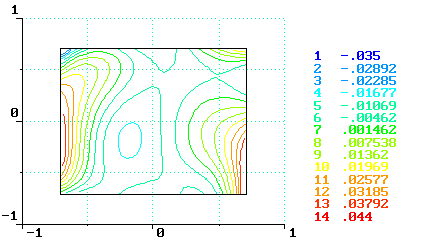
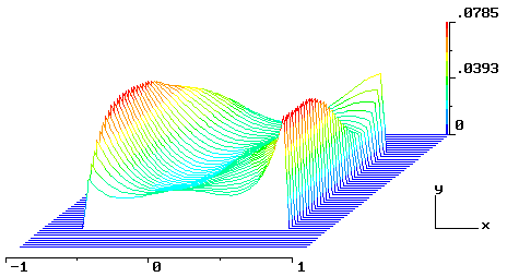
Fig. 4 Reconctracted wavefront topography presented at planar and 3-d plots.
| 194 x 130 microns plane |
Regular errors:
| D= .000 | LX= 2.811 | LY= .053 | C= 2.045 | RMS(W)= .024 | |
| A= .104 | FIA= 81.477 | RMS(W-A)= .011 | FA= .787 | ||
| B0= -.020 | RZ= .083 | RMS(W-Z)= .016 | FZ= .561 | ||
| B2=.039 | |||||
| B4= .117 | |||||
| C= .022 | FIC= 50.186 | RMS(W-C)= .023 | FC= .014 |
Local errors:
| R= .077 | RMS(M)= .012 |
Parameters of surface:
| RMS | MIN | MAX | R | STRL | STRH |
| .024 | -.036 | .076 | .112 | .978 | .993 |
| X : | -.200 | .680 |
| Y : | .480 | -.440 |
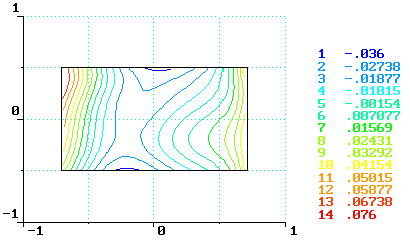
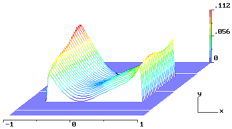
Fig. 5 Reconctracted wavefront topography presented at planar and 3-d plots.
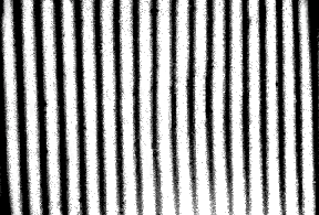
Fig. 6 Interferogram of the surface S1.
Such thorough control on each step of production can guarantee that all parameters of the item meet specifications required by customer and that the device will operate in a proper way.