0
  • 聊天消息
  • 系统消息
  • 评论与回复
登录后你可以
  • 下载海量资料
  • 学习在线课程
  • 观看技术视频
  • 写文章/发帖/加入社区
创作中心

完善资料让更多小伙伴认识你,还能领取20积分哦,立即完善>

3天内不再提示

TMS320C6711D 浮点数字信号处理器

数据:

描述

TMS320C67x ??的DSP(包括TMS320C6711,TMS320C6711B,TMS320C6711C,TMS320C6711D设备)构成浮点DSP家族在TMS320C6000? DSP平台。在C6711,C6711B,C6711C和C6711D设备都是基于高性能,先进的超长指令字(VLIW)架构的德州仪器(TI)开发,使这些DSP的多通道多功能应用的绝佳选择。

C6711D器件的时钟频率为200 MHz,时钟速率高达1200万次(MFLOPS),时钟频率为250 MHz,最高可达1500 MFLOPS,高效DSP编程挑战的有效解决方案。 C6711D DSP具有高速控制器的操作灵活性和阵列处理器的数字能力。该处理器具有32个32位字长的通用寄存器和8个高度独立的功能单元。八个功能单元提供四个浮点/定点ALU,两个定点ALU和两个浮点/定点乘法器。 C6711D每个周期可以产生两个MAC,总共400 MMACS。

C6711D DSP还具有专用硬件逻辑,片上存储器和其他片上外设。

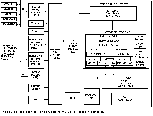
< p> C6711D设备使用基于缓存的两级架构,并具有功能强大且多样化的外设集。 1级程序高速缓存(L1P)是32-Kbit直接映射高速缓存,1级数据高速缓存(L1D)是32-Kbit 2路组关联高速缓存。 2级内存/高速缓存(L2)由512-Kbit的内存空间组成,在程序和数据空间之间共享。 L2内存可以配置为映射内存,缓存或两者的组合。外围组包括两个多信道缓冲串行端口(McBSP的),两个通用定时器,主机端口接口(HPI),和一个无缝外部存储器接口(EMIF)能够连接到SDRAM,SBSRAM和异步外围设备。

C6711D有一套完整的开发工具,包括:一个新的C编译器,一个简化编程和调度的汇编优化器,以及一个Windows?调试器接口,用于查看源代码执行情况。

特性

  • Excellent-Price/Performance Floating-Point Digital Signal Processor (DSP):
      TMS320C6711D
    • Eight 32-Bit Instructions/Cycle
    • 167-, 200-, 250-MHz Clock Rates
    • 6-, 5-, 4-ns Instruction Cycle Time
    • 1000, 1200, 1500 MFLOPS
  • Advanced Very Long Instruction Word (VLIW) C67x™ DSP Core
    • Eight Highly Independent Functional Units:
      • Four ALUs (Floating- and Fixed-Point)
      • Two ALUs (Fixed-Point)
      • Two Multipliers (Floating- and Fixed-Point)
    • Load-Store Architecture With 32 32-Bit General-Purpose Registers
    • Instruction Packing Reduces Code Size
    • All Instructions Conditional
  • Instruction Set Features
    • Hardware Support for IEEE Single-Precision and Double-Precision Instructions
    • Byte-Addressable (8-, 16-, 32-Bit Data)
    • 8-Bit Overflow Protection
    • Saturation
    • Bit-Field Extract, Set, Clear
    • Bit-Counting
    • Normalization
  • L1/L2 Memory Architecture
    • 32K-Bit (4K-Byte) L1P Program Cache (Direct Mapped)
    • 32K-Bit (4K-Byte) L1D Data Cache (2-Way Set-Associative)
    • 512K-Bit (64K-Byte) L2 Unified Mapped RAM/Cache (Flexible Data/Program Allocation)
  • Device Configuration
    • Boot Mode: HPI, 8-, 16-, 32-Bit ROM Boot
    • Endianness: Little Endian, Big Endian
  • Enhanced Direct-Memory-Access (EDMA) Controller (16 Independent Channels)
  • 32-Bit External Memory Interface (EMIF)
    • Glueless Interface to Asynchronous Memories: SRAM and EPROM
    • Glueless Interface to Synchronous Memories: SDRAM and SBSRAM
    • 256M-Byte Total Addressable External Memory Space
  • 16-Bit Host-Port Interface (HPI)
  • Two Multichannel Buffered Serial Ports (McBSPs)
    • Direct Interface to T1/E1, MVIP, SCSA Framers
    • ST-Bus-Switching Compatible
    • Up to 256 Channels Each
    • AC97-Compatible
    • Serial-Peripheral-Interface (SPI) Compatible (Motorola™)
  • Two 32-Bit General-Purpose Timers
  • Flexible Software Configurable PLL-Based Clock Generator Module
  • A Dedicated General-Purpose Input/Output (GPIO) Module With 5 Pins
  • IEEE-1149.1 (JTAG) Boundary-Scan-Compatible
  • 272-Pin Ball Grid Array (BGA) Package (GDP and ZDP Suffixes)
  • CMOS Technology
    • 0.13-µm/6-Level Copper Metal Process
  • 3.3-V I/O, 1.4-V Internal (-250)
  • 3.3-V I/O, 1.20-V Internal

TMS320C67x and C67x are trademarks of Texas Instruments.
Motorola is a trademark of Motorola, Inc.
All trademarks are the property of their respective owners.
IEEE Standard 1149.1-1990 Standard-Test-Access Port and Boundary Scan Architecture.
These values are compatible with existing 1.26V designs.
TMS320C6000 is a trademark of Texas Instruments.
Windows is a registered trademark of the Microsoft Corporation.
Throughout the remainder of this document, the TMS320C6711D shall be referred to as its individual full device part number or abbreviated as C6711D or 11D.

参数 与其它产品相比 其他 C6000 DSP

 
DSP
TMS320C6711D
1 C67x    

方框图 (1)


技术文档

数据手册(1)
元器件购买 TMS320C6711D 相关库存