


SEPIC Backlight LED Driver,SEPIC背光LED驱动器
Abstract: This is a reference design for a SEPIC/linear LED-display backlight driver for eight parallel strings of 8 WLEDs (white LEDs) at70mA/string. The dimming ratio is 4000:1. The input voltage is 16V to 36V with 50V transients. The design combines a SEPIC switching power supply with adaptive feedback and linear current sinks for high dimming ratios. The MAX16809 16-channel LED driver is featured.
Overview
This reference design is an LED backlight driver for a 12in TFT display. The electrical input requirements and output capabilities follow:
| VIN (power): | 16V (at 1092mA) to 36V (at 476mA); tolerant to 50V transients |
| VBIAS: | 3.3V at 50mA |
| PWMIN: | 250Hz pulse train; 1µsec (min) pulse; > 3.1V at 0mA; < 0.3V at 10mA |
| VLED config.: | 8 LEDs (2.9V to 3.75V) in series (31V, max); eight parallel strings; 70mA per string |
More detailed image (PDF, 51.64kB)
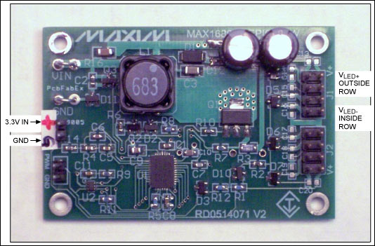
Figure 1. The driver board features the MAX16809.
More detailed image (PDF, 14.83kB)
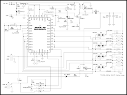
Figure 2. Schematic of the driver design.
Brief Circuit Description
This reference design uses the MAX16809 as a central controller for a SEPIC power supply and a 16-port LED driver. The 16 ports are grouped in pairs to drive eight parallel strings of LEDs. SEPIC power supplies allow the input voltage to be greater, or lesser, than the output power supply. This is a preferred topology because of the input and output voltage variations that occur with LEDs in automotive environments. The SEPIC power supply operates at a frequency of 200kHz, which is fast enough for small power components and yet slow enough to prevent overheating the switching MOSFET. The coupled inductor, L1, which is made by Coilcraft®, contains both the primary and secondary inductances needed by a SEPIC power supply. The use of a coupled inductor allows the design to accept half the inductance that a design with two discrete inductors would require.
The PCB has been modified with leaded, low-ESR, electrolytic capacitors. These capacitors are necessary to absorb the inductive energy of the power supply when the PWM signal shuts down. The output voltage for the LED strings is available through two, 8-pin headers: VLED+ is on the outer row of the headers, and the VLED- pins are on the inner row of the headers. Pads for output filter capacitors are available if desired; they are not populated in this design. The Q2-D2-R8 circuit provides slope compensation for the current-mode PWM controller. This circuit, which follows the RTCT ramp voltage, injects current into R7, thus creating a ramp voltage that helps prevent subharmonic oscillation of the controller at duty cycles greater than 50% (when the input voltage is at the lower end).
The SEPIC feedback path has two modes: adaptive and resting. The adaptive mode (when the PWM signal is high) will "diode-OR" the outputs so that the lowest driver voltage (largest series LED string voltage) is regulated to about 700mV. This provides enough headroom for proper operation of the LED driver. Other LED strings will have a lower series voltage and thus those drivers have greater headroom. Adaptive mode minimizes the power dissipation caused by the linear LED drivers. For this approach to work, while the absolute LED forward voltage is not critical, the relative forward voltage between LEDs must be matched to within 200mV of each other. To dissipate the heat, the MAX16801 must have a good thermal connection to large copper planes using thermal vias beneath the exposed pad of the package. In this board, the bottom plane provides cooling to the IC, but multiplane grounds with larger surface areas will dissipate the heat even better.
In the resting mode (when the PWM signal is low), VLED is regulated like a conventional power supply, and the voltage rises to a value that will guarantee operation for very short pulses. Since the power-supply magnetics cannot charge quickly enough for short pulses, all of the energy must originate from the output capacitors. The resting mode ensures that the capacitors are charged enough to sustain this energy until the magnetics can respond.
Zener diode, D10, provides overvoltage protection to the circuit. If an LED string becomes disconnected, the adaptive voltage control would attempt to increase VLED to satisfy the 700mV requirement. D10 limits the output voltage to 35.5V. While this voltage will not harm the circuit, the resulting power dissipation in the LED drivers will overheat the MAX16809. The chip's internal circuitry will then power the drivers down until the temperature is reduced. The resulting effect is LED blinking.
The LED drivers are set to 35mA through R5 (511Ω). By paralleling two drivers per LED string, the IC provides 70mA per string.
A Schmitt-triggered inverter, U2, is configured as an oscillator to provide a clock to the SPI input of the MAX16801. Since DIN is connected high, a string of "1s" is clocked into an internal register which enables all the LED drivers. U2 also inverts the PWM signal to meet the requirements of the MAX16809's OE# input.
The Q3-D11-R16 circuit preregulates input power to the MAX16809's PWM controller. This simple linear regulator reduces the input voltage to 12V, which allows full IC operation and MOSFET gate drive. Input power for the LED drivers of the IC (V+) must come from an external 3.3V power supply. (This is an alteration to the original PCB.) The LED drivers present a maximum load of 50mA.
Test and Performance Results
More detailed image (PDF, 34.14kB)
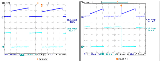
Figure 3. MOSFET current and voltages with VIN =18V and with VIN = 36V. 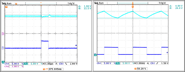
More detailed image (PDF, 34.23kB)
Figure 4. VLED with 1µs pulse and with a 2ms pulse. VLED alternates between resting mode and adaptive mode. 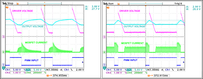
More detailed image (PDF, 40.38kB)
Figure 5. LED driver voltage, VLED voltage, and MOSFET current with 1.5msec and 3.5msec pulses. The LED driver voltage is high until VLED reaches adaptive mode.
Temperature Measurements
The following temperatures were measured using eight 400Ω resistors as loads:
| VIN Ambient |
16VDC +20°C |
| TU1 | +59°C |
| TQ1 | +56°C |
| TL1 | +65°C |
| TQ3 | +46°C |
| TD1 | +60°C |
| VIN Ambient |
36VDC +20°C |
| TU1: | +54°C |
| TQ1: | +48°C |
| TL1: | +61°C |
| TQ3: | +57°C |
| TD1: | +56°C |
Power-Up Procedure
- Attach a string of 8 LEDs to each output. The positive side of the LEDs must be attached to the outside pin of the output header; the negative side of the LEDs must be attached to the inside pin of the output header.
- Attach an unpowered 3.3V power supply to J5. Be sure to match the correct polarity.
- Attach an unpowered 18V to 36V (2A rating) to the input wire loops. Be sure to match the correct polarity.
- Turn on the power to the circuit. Sequencing is not critical.
- Apply a 250Hz pulse wave to J4. The pulse wave must vary from 0V to 3.3V and the duty cycle can go from 0.1% to 100%.
- Large vias on either side of the current-sense resistor, R3, allow for low-noise probing using a ground coil and a single-ended scope probe.


 工商网监
工商网监
用户评论
共 条评论