
| Current consumption (mA) | 106 |
| Frequency (Min) (MHz) | 2300 |
| Frequency (Max) (MHz) | 2900 |
| Gain (Typ) (dB) | 18 |
| Impedance match (Ohms) | 50 |
| Noise figure (Typ) (dB) | 3.2 |
| Number of channels (#) | 1 |
| Operating temperature range (C) | -40 to 105 |
| Output enable | Yes |
| Output IP3 (Typ) (dBm) | 33 |
| P1dB (Typ) (dBm) | 18 |
| Type | Active Balun |
| Rating | Catalog |
| Power down current | 10 mA |
- Single-Channel, Differential Input to Single-Ended Output RF Gain Block Amplifier
- 18-dB Typical Gain Across the Band
- 3.5-dB Noise Figure
- 35-dBm OIP3
- 18-dBm Output P1dB
- 375-mW Power Consumption on 3.3-V Single Supply
- Up to 105°C TC Operating Temperature
The LMH9126 is high-performance, single-channel, differential input to single-ended output transmit RF gain block amplifier supporting 2.6-GHz center frequency band. The device is well suited to support requirements for the next generation 5G AAS or small cell applications while driving the input of a power amplifier (PA). The RF amplifier provides 18-dB typical gain with good linearity performance of 35-dBm output IP3, while maintaining less than 4-dB noise figure across the whole 1-dB bandwidth. The device is internally matched for 100-Ω differential input impedance providing easy interface with an RF-sampling or Zero-IF analog front-end (AFE) at the input. Also, the device is internally matched for 50-Ω single-ended output impedance required for easy interface with a post-amplifier, SAW filter, or PA.
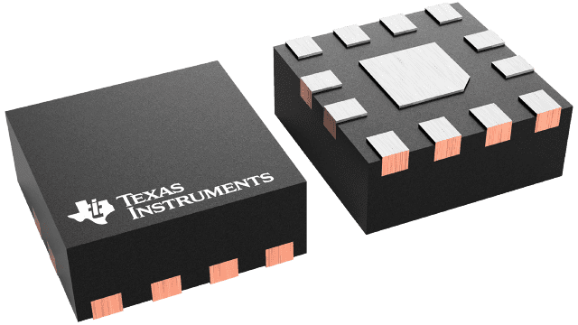
Operating on a single 3.3-V supply, the device consumes only 375 mW of active power making it suitable for high-density 5G massive MIMO applications. Also, the device is available in a space saving 2-mm × 2-mm, 12-pin QFN package. The device is rated for an operating temperature of up to 105°C to provide a robust system design. There is a 1.8-V JEDEC compliant power down pin available for fast power down and power up of the device suitable for time division duplex (TDD) systems.


