

| Regulated outputs (#) | 6 |
| Vin (Min) (V) | 2.5 |
| Vin (Max) (V) | 6 |
| Iout (Max) (A) | 1.2 |
| Rating | Catalog |
| LDO | 3 |
| Iq (Typ) (mA) | 0.085 |
| Features | Comm Control, Power Good, Power Sequencing |
| Processor name | PXA |
| Processor supplier | Marvell |
| Shutdown current (ISD) (Typ) (uA) | 23 |
| Switching frequency (Typ) (kHz) | 1500 |
| Configurability | Hardware configurable, Software configurable |
- 1.2-A, 97% Efficient Step-Down Converter for
System Voltage (VDCDC1) - 1-A, Up to 95% Efficient Step-Down Converter for
Memory Voltage (VDCDC2) - 900-mA, 90% Efficient Step-Down Converter for
Processor Core (VDCDC3) - 30-mA LDO and Switch for Real-Time Clock
(VRTC) - 2 × 200-mA General-Purpose LDO
- Dynamic Voltage Management for Processor Core
- Preselectable LDO Voltage Using Two Digital
Input Pins - Externally Adjustable Reset Delay Time
- Battery Backup Functionality
- Separate Enable Pins for Inductive Converters
- I2C-Compatible Serial Interface
- 85-μA Quiescent Current
- Low-Ripple PFM Mode
- Thermal Shutdown Protection
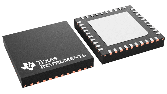
- 40-Pin 6-mm × 6-mm VQFN Package
The TPS65021 device is an integrated power management IC for applications powered by one Li-Ion or Li-Polymer cell, and which requires multiple power rails. The TPS65021 device provides three highly efficient, step-down converters targeted at providing the core voltage, peripheral, I/O, and memory rails in a processor-based system. All three step-down converters enter a low-power mode at light load for maximum efficiency across the widest possible range of load currents.
The TPS65021 device also integrates two general-purpose 200-mA LDO voltage regulators, which are enabled with an external input pin. Each LDO operates with an input voltage range from 1.5 V to 6.5 V, thus allowing them to be supplied from one of the step-down converters or directly from the battery. The default output voltage of the LDOs can be digitally set to 4 different voltage combinations using the DEFLDO1 and DEFLDO2 pins. The serial interface can be used for dynamic voltage scaling, masking interrupts, or for disabling or enabling and setting the LDO output voltages. The interface is compatible with both the fast and standard mode I2C specifications, allowing transfers at up to 400 kHz. The TPS65021 device is available in a 40-pin (RHA) VQFN package, and operates over a free-air temperature of ?40°C to +85°C.


