


| Regulated outputs (#) | 7 |
| Vin (Min) (V) | 2.7 |
| Vin (Max) (V) | 5.5 |
| Iout (Max) (A) | 1.2 |
| Rating | Catalog |
| LDO | 4 |
| Features | Comm Control, Power Sequencing |
| Processor name | OMAP |
| Processor supplier | Texas Instruments |
| Switching frequency (Typ) (kHz) | 3200 |
| Configurability | Factory programmable |
- Three Step-Down Converters:
- Up to 1.2 A of Output Current for VDD1
- TPS65921B Supports VDD1 up to 1.2 A
- TPS65921B1 Supports VDD1 up to 1.4 A (Necessary for 1-GHz Operation)
- SmartReflex Dynamic Voltage Management
- 3.2-MHz Fixed Frequency Operation
- VIN Range from 2.7 to 4.5 V
- Typical 30 μA Quiescent per Converter
- Up to 1.2 A of Output Current for VDD1
- Four General-Purpose Configurable LDOs:
- Dynamic Voltage Scaling
- 220-mA Maximum Current for One LDO
- VIN Range from 2.7 to 4.5 V
- 2 LDOs With Low Noise and High PSRR
- RTC With Alarm Wake-Up Mechanism
- Clock Management
- 32-kHz Crystal Oscillator
- Clock Slicer for 26, 19.2, and 38.4 MHz
- HF Clock Output Buffer
- USB:
- USB HS 2.0 Transceiver
- USB 1.3 OTG-Compliant
- 12-Bit ULPI 1.1 Interface
- USB Power Supply (5-V CP for VBUS)
- Control
- High-Speed I2C Interface
- All Resource Configurable by I2C
- Keypad Interface up to 8 × 8
- 10-Bit A/D Converter
- Hot-Die, Thermal Shutdown Protection
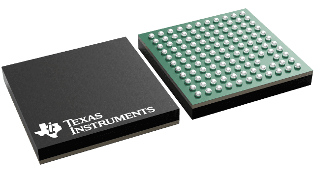
- μ*BGA 120 Balls ZQZ
The TPS65921 device is a highly integrated power-management circuit (IC) that supports the power and peripheral requirements of the OMAP application processors. The device contains power management, a universal serial bus (USB) high-speed (HS) transceiver, an analog-to-digital converter (ADC), a real-time clock (RTC), a keypad interface, and an embedded power control (EPC). The power portion of the device contains three buck converters, two controllable by a dedicated SmartReflex class-3 interface, multiple low-dropout (LDO) regulators, an EPC to manage the power-sequencing requirements of OMAP, and an RTC module. The USB module provides an HS 2.0 transceiver suitable for direct connection to the OMAP universal transceiver macrocell interface (UTMI) + low pin interface (ULPI) with an integrated charge pump (CP).
The device also provides auxiliary modules: ADC, keypad interface, and general-purpose inputs/outputs (GPIOs) muxed with the JTAG functions. The keypad interface implements a built-in scanning algorithm to decode hardware-based key presses and to reduce software use, with multiple additional GPIOs that can be used as interrupts when they are configured as inputs.