


| DSP | 1 C64x |
| DSP MHz (Max) | 300 |
| CPU | 32-/64-bit |
| Operating system | DSP/BIOS |
| PCIe | 1 PCI |
| Rating | Catalog |
| Operating temperature range (C) | 0 to 90 |
- Low-Cost, High-Performance Fixed-Point DSP – TMS320C6411
- 3.33-ns Instruction Cycle Time
- 300-MHz Clock Rate
- Eight 32-Bit Instructions/Cycle
- Twenty-Eight Operations/Cycle
- 2400 MIPS
- Fully Software-Compatible With TMS320C62x?
- VelociTI.2? Extensions to VelociTI? Advanced Very-Long-Instruction-Word (VLIW) TMS320C64x? DSP Core
- Eight Highly Independent Functional Units With VelociTI? Extensions:
- Six ALUs (32-/40-Bit), Each Supports Single 32-Bit, Dual 16-Bit, or Quad 8-Bit Arithmetic per Clock Cycle
- Two Multipliers Support Four 16 x 16-Bit Multiplies (32-Bit Results) per Clock Cycle or Eight 8 x 8-Bit Multiplies (16-Bit Results) per Clock Cycle
- Non-Aligned Load-Store Architecture
- 64 32-Bit General-Purpose Registers
- Instruction Packing Reduces Code Size
- All Instructions Conditional
- Eight Highly Independent Functional Units With VelociTI? Extensions:
- Instruction Set Features
- Byte-Addressable (8-/16-/32-/64-Bit Data)
- 8-Bit Overflow Protection
- Bit-Field Extract, Set, Clear
- Normalization, Saturation, Bit-Counting
- VelociTI.2? Increased Orthogonality
- L1/L2 Memory Architecture
- 128K-Bit (16K-Byte) L1P Program Cache (Direct Mapped)
- 128K-Bit (16K-Byte) L1D Data Cache (2-Way Set-Associative)
- 2M-Bit (256K-Byte) L2 Unified Mapped RAM/Cache (Flexible RAM/Cache Allocation)
- 32-Bit External Memory Interface (EMIF)
- Glueless Interface to Asynchronous Memories (SRAM and EPROM) and Synchronous Memories (SDRAM, SBSRAM, ZBT SRAM, and FIFO)
- 512M-Byte Total Addressable External Memory Space
- Enhanced Direct-Memory-Access (EDMA) Controller (64 Independent Channels)
- Host-Port Interface (HPI)
- User-Configurable Bus Width (32-/16-Bit)
- Access to Entire Memory Map
- 32-Bit/33-MHz, 3.3-V Peripheral Component Interconnect (PCI) Master/Slave Interface Conforms to PCI Specification 2.2
- Access to Entire Memory Map
- Three PCI Bus Address Registers:
Prefetchable Memory
Non-Prefetchable Memory I/O - Four-Wire Serial EEPROM Interface
- PCI Interrupt Request Under DSP Program Control
- DSP Interrupt Via PCI I/O Cycle
- Two Multichannel Buffered Serial Ports (McBSPs)
- Direct Interface to T1/E1, MVIP, SCSA Framers
- ST-Bus-Switching Compatible
- Up to 256 Channels Each
- AC97-Compatible
- Serial Peripheral Interface (SPI) Compatible (Motorola?)
- Three 32-Bit General-Purpose Timers
- Sixteen General-Purpose I/O (GPIO) Pins
- Programmable Interrupt/Event Generation Modes
- Flexible PLL Clock Generator
- IEEE-1149.1 (JTAG
 ) Boundary-Scan-Compatible
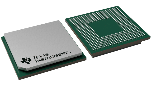
 - 532-Pin Ball Grid Array (BGA) Package (GLZ, ZLZ and CLZ Suffixes), 0.8-mm Ball Pitch
- 0.13-μm/6-Level Copper Metal Process
- CMOS Technology
- 3.3-V I/Os, 1.2-V Internal
TMS320C62x, VelociTI.2, VelociTI, and TMS320C64x are trademarks of Texas Instruments.
Motorola is a trademark of Motorola, Inc. IEEE Standard 1149.1-1990 Standard-Test-Access Port and Boundary Scan Architecture.
TMS320C6000, C64x, and C6000 are trademarks of Texas Instruments.
Windows is a registered trademark of the Microsoft Corporation.
Other trademarks are the property of their respective owners.
The TMS320C64x? DSPs (including the TMS320C6411 device) are the highest-performance fixed-point DSP generation in the TMS320C6000? DSP platform. The TMS320C6411 (C6411) device is based on the second-generation high-performance, advanced VelociTI? very-long-instruction-word (VLIW) architecture (VelocTI.2?) developed by Texas Instruments (TI), making these DSPs an excellent choice for multichannel and multifunction applications. The C64x? is a code-compatible member of the C6000? DSP platform.
With performance of up to 2400 million instructions per second (MIPS) at a clock rate of 300 MHz, the C6411 device offers cost-effective solutions to high-performance DSP programming challenges. The C6411 DSP possesses the operational flexibility of high-speed controllers and the numerical capability of array processors. The C64x? DSP core processor has 64 general-purpose registers of 32-bit word length and eight highly independent functional units?two multipliers for a 32-bit result and six arithmetic logic units (ALUs)?with VelociTI.2? extensions. The VelociTI.2? extensions in the eight functional units include new instructions to accelerate the performance in key applications and extend the parallelism of the VelociTI? architecture. The C6411 can produce four 16-bit multiply-accumulates (MACs) per cycle for a total of 600 million MACs per second (MMACS), or eight 8-bit MACs per cycle for a total of 2400 MMACS. The C6411 DSP also has application-specific hardware logic, on-chip memory, and additional on-chip peripherals similar to the other C6000? DSP platform devices.
The C6411 uses a two-level cache-based architecture and has a powerful and diverse set of peripherals. The Level 1 program cache (L1P) is a 128-Kbit direct mapped cache and the Level 1 data cache (L1D) is a 128-Kbit 2-way set-associative cache. The Level 2 memory/cache (L2) consists of a 2-Mbit memory space that is shared between program and data space. L2 memory can be configured as mapped memory or combinations of cache (up to 256K bytes) and mapped memory. The peripheral set includes two multichannel buffered serial ports (McBSPs); three 32-bit general-purpose timers; a user-configurable 16-bit or 32-bit host-port interface (HPI16/HPI32); a peripheral component interconnect (PCI); a general-purpose input/output port (GPIO) with 16 GPIO pins; and a glueless external memory interface (32-bit EMIF), which is capable of interfacing to synchronous and asynchronous memories and peripherals.
The C6411 has a complete set of development tools which includes: a new C compiler, an assembly optimizer to simplify programming and scheduling, and a Windows? debugger interface for visibility into source code execution.


