



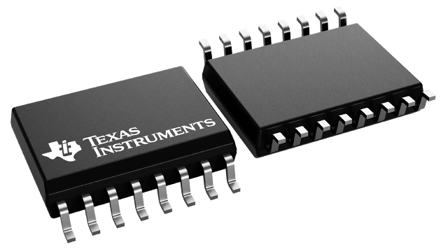

| Number of receivers | 4 |
| Number of transmitters | 0 |
| Supply voltage (Nom) (V) | 5 |
| Signaling rate (Max) (Mbps) | 10 |
| Fault protection (V) | -10 to 15 |
| Common mode range | -7 to 12 |
| Number of nodes | 32 |
| Isolated | No |
| ICC (Max) (mA) | 20 |
| Rating | Catalog |
| Operating temperature range (C) | -40 to 85 |
- Meets or Exceeds the EIA Standards RS-422-A,
RS-423-A, RS-485, and CCITT Recommendation V.11 - Designed to Operate With Pulse Durations
as Short as 20 ns - Designed for Multipoint Transmission on
Long Bus Lines in Noisy Environments - Input Sensitivity . . . ±200 mV
- Low-Power Consumption . . . 20 mA Max
- Open-Circuit Fail-Safe Design
- Common-Mode Input Voltage Range of
–7 V to 12 V - Pin Compatible With SN75175 and LTC489
LinBiCMOS is a trademark of Texas Instruments.
The SN65LBC175 and SN75LBC175 are monolithic, quadruple, differential line receivers with 3-state outputs designed to meet the requirements of the EIA standards RS-422-A, RS-423-A, RS-485, and CCITT Recommendation V.11. The devices are optimized for balanced multipoint bus transmission at data rates up to and exceeding 10 million bits per second. The receivers are enabled in pairs, with an active-high enable input. Each differential receiver input features high impedance, hysteresis for increased noise immunity, and sensitivity of ±200 mV over a common-mode input voltage range of 12 V to ?7 V. The fail-safe design ensures that when the inputs are open-circuited, the outputs are always high. Both devices are designed using the TI proprietary LinBiCMOS.technology allowing low power consumption, high switching speeds, and robustness.
These devices offer optimum performance when used with the SN75LBC172 or SN75LBC174 quadruple line drivers. The SN65LBC175 is available in the 16-pin DIP (N), small-outline package (D), and the wide small-outline package (DW). The SN75LBC175 is available in the 16-pin DIP (N) and the small-outline package (D).
The SN65LBC175 is characterized over the industrial temperature range of ?40°C to 85°C. The SN75LBC175 is characterized for operation over the commercial temperature range of 0°C to 70°C.