


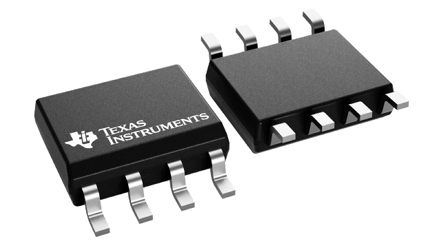

| Number of receivers | 1 |
| Number of transmitters | 1 |
| Duplex | Half |
| Supply voltage (Nom) (V) | 5 |
| Signaling rate (Max) (Mbps) | 30 |
| Fault protection (V) | -10 to 15 |
| Common mode range | -7 to 12 |
| Number of nodes | 32 |
| Isolated | No |
| ICC (Max) (mA) | 15 |
| Rating | Automotive, Catalog |
| Operating temperature range (C) | -40 to 125, -40 to 85 |
- Designed for Signal Rates Up to 30
 Mbps
Mbps - Bus-Pin ESD Protection Exceeds 12 kV HBM
- Compatible With ANSI Standard TIA/EIA-485-A and ISO 8482:1987(E)
- Low Skew
- Designed for Multipoint Transmission on Long Bus Lines in Noisy Environments
- Very Low Disabled Supply-Current Requirements...700 μA Maximum
- Common Mode Voltage Range of -7 V to 12 V
- Thermal-Shutdown Protection
- Driver Positive and Negative Current Limiting
- Open-Circuit Fail-Safe Receiver Design
- Receiver Input Sensitivity...±200 mV Max
- Receiver Input Hysteresis...50 mV Typ
- Glitch-Free Power-Up and Power-Down Protection
- Available in Q-Temp Automotive
High Reliability Automotive Applications
Configuration Control / Print Support
Qualification to Automotive Standards
LinBiCMOS and LinASIC are trademarks of Texas Instruments.  Signaling rate by TIA/EIA-485-A definition restrict transition times to 30% of the bit length, and much higher signaling rates may be achieved without this requirement as displayed in the TYPICAL CHARACTERISTICS of this device.
The SN65LBC176A, SN65LBC176AQ, and SN75LBC176A differential bus transceivers are monolithic, integrated circuits designed for bidirectional data communication on multipoint bus-transmission lines. They are designed for balanced transmission lines and are compatible with ANSI standard TIA/EIA-485-A and ISO 8482. The A version offers improved switching performance over its predecessors without sacrificing significantly more power.
The SN65LBC176A, SN65LBC176AQ, and SN75LBC176A combine a 3-state, differential line driver and a differential input line receiver, both of which operate from a single 5-V power supply. The driver and receiver have active-high and active-low enables, respectively, which can externally connect together to function as a direction control. The driver differential outputs and the receiver differential inputs connect internally to form a differential input/output (I/O) bus port that is designed to offer minimum loading to the bus whenever the driver is disabled or VCC = 0. This port features wide positive and negative common-mode voltage ranges, making the device suitable for party-line applications. Very low device supply current can be achieved by disabling the driver and the receiver.