




| Drivers per package | 0 |
| Receivers per package | 4 |
| Logic voltage (Min) (V) | 5 |
| Data rate (Max) (kbps) | 1000 |
| Main supply voltage (Nom) (V) | 5 |
| ESD HBM (kV) | 0 |
| Rating | Catalog |
| Operating temperature range (C) | 0 to 70 |
- Meet or Exceed the Requirements of TIA/EIA-232-F and ITU Recommendation V.28
- Low Supply Current...420 uA Typ
- Preset On-Chip Input Noise Filter
- Built-in Input Hysteresis
- Response and Threshold Control Inputs
- Push-Pull Outputs
- Functionally Interchangeable and Pin-to-Pin Compatible With Texas Instruments SN75189/SN75189A and Motorola MC1489/MC1489A
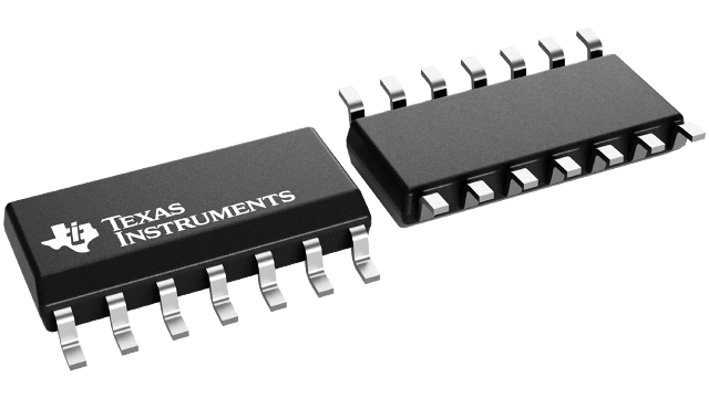
- Package Options Include Plastic Small-Outline (D) and Shrink Small-Outline (DB) Packages, and Standard Plastic (N) DIP
The SN75C189 and SN75C189A are low-power, bipolar, quadruple line receivers that are used to interface data terminal equipment (DTE) with data circuit-terminating equipment (DCE). These devices have been designed to conform to TIA/EIA-232-F.
The SN75C189 has a 0.33-V typical hysteresis, compared with 0.97 V for the SN75C189A. Each receiver has provision for adjustment of the overall input threshold levels. This is achieved by choosing external series resistors and voltages to provide bias levels for the response-control pins. The output is in the high logic state if the input is open circuit or shorted to ground.
These devices have an on-chip filter that rejects input pulses of less than 1-us duration. An external capacitor can be connected from the control pins to ground to provide further input noise filtering for each receiver.
The SN75C189 and SN75C189A have been designed using low-power techniques in a bipolar technology. In most applications, these receivers interface to single inputs of peripheral devices such as UARTs, ACEs, or microprocessors. By using sampling, such peripheral devices usually are insensitive to the transition times of the input signals. If this is not the case, or for other uses, it is recommended that the SN75C189 and SN75C189A outputs be buffered by single Schmitt input gates or single gates of the HCMOS, ALS, or 74F logic families.
The SN75C189 and SN75C189A are characterized for operation from 0°C to 70°C.