



| Number of SRC channels | 2 |
| Digital audio interface | AES/EBU, S/PDIF |
| Dynamic range (dB) | 144 |
| Digital supply (up to 5 V) (V) | 1.65 - 1.95, 3 - 3.6 |
| THD+N (dB) | -140 |
| Control mode | SW (SPI), H/W |
| Power supply (V) | 1.8, 3.3 |
| Control interface | SPI, I2C |
| Audio data format | Normal, I2S |
| Rating | Catalog |
| Operating temperature range (C) | -40 to 85 |
- Two-Channel Asynchronous Sample Rate Converter (SRC)
- Dynamic Range with –60dB Input (A-Weighted): 144dB typical
- Total Harmonic Distortion and Noise (THD+N) with Full-Scale Input: –140dB typical
- Supports Audio Input and Output Data Word Lengths Up to 24 Bits
- Supports Input and Output Sampling Frequencies Up to 216kHz
- Automatic Detection of the Input-to-Output Sampling Ratio
- Wide Input-to-Output Conversion Range:
16:1 to 1:16 Continuous - Excellent Jitter Attenuation Characteristics
- Digital De-Emphasis Filtering for 32kHz, 44.1kHz, and 48kHz Input Sampling Rates
- Digital Output Attenuation and Mute Functions
- Output Word Length Reduction
- Status Registers and Interrupt Generation for Sampling Ratio and Ready Flags
- Digital Audio Interface Transmitter (DIT)
- Supports Sampling Rates Up to 216kHz
- Includes Differential Line Driver and
CMOS Buffered Outputs - Block-Sized Data Buffers for Both Channel Status and User Data
- Status Registers and Interrupt Generation for Flag and Error Conditions
- User-Selectable Serial Host Interface: SPI or Philips I2C?
- Provides Access to On-Chip Registers and Data Buffers
U.S. Patent No. 7,262,716
- Digital Audio Interface Receiver (DIR)
- PLL Lock Range Includes Sampling Rates from 20kHz to 216kHz
- Includes Four Differential Input Line Receivers and an Input Multiplexer
- Bypass Multiplexer Routes Line Receiver Outputs to Line Driver and Buffer Outputs
- Block-Sized Data Buffers for Both Channel Status and User Data
- Automatic Detection of Non-PCM Audio Streams (DTS CD/LD and IEC 61937 formats)
- Audio CD Q-Channel Sub-Code Decoding and Data Buffer
- Status Registers and Interrupt Generation for Flag and Error Conditions
- Low Jitter Recovered Clock Output
- Two Audio Serial Ports (Ports A and B)
- Synchronous Serial Interface to External Signal Processors, Data Converters, and Logic
- Slave or Master Mode Operation with Sampling Rates up to 216kHz
- Supports Left-Justified, Right-Justified, and Philips I2S? Data Formats
- Supports Audio Data Word Lengths Up to
24 Bits
- Four General-Purpose Digital Outputs
- Multifunction Programmable Via Control Registers
- Extensive Power-Down Support
- Functional Blocks May Be Disabled Individually When Not In Use
- Operates From +1.8V Core and +3.3V I/O Power Supplies
- Packages:
- QFN-40
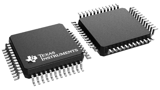
- Small TQFP-48 Package, Compatible with the SRC4382 and DIX4192
The SRC4392 is a highly-integrated CMOS device designed for use in professional and broadcast digital audio systems. The SRC4392 combines a high-performance, two-channel, asynchronous sample rate converter (SRC) with a digital audio interface receiver (DIR) and transmitter (DIT), two audio serial ports, and flexible distribution logic for interconnection of the function block data and clocks.
The DIR and DIT are compatible with the AES3, S/PDIF, IEC 60958, and EIAJ CP-1201 interface standards. The audio serial ports, DIT, and SRC may be operated at sampling rates up to 216kHz. The DIR lock range includes sampling rates from 20kHz to 216kHz.
The SRC4392 is configured using on-chip control registers and data buffers, which are accessed through either a 4-wire serial peripheral interface (SPI) port, or a 2-wire Philips I2C bus interface. Status registers provide access to a variety of flag and error bits, which are derived from the various function blocks. An open drain interrupt output pin is provided, and is supported by flexible interrupt reporting and mask options via control register settings. A master reset input pin is provided for initialization by a host processor or supervisory functions.
The SRC4392 requires a +1.8V core logic supply, in addition to a +3.3V supply for powering portions of the DIR, DIT, and line driver and receiver functions. A separate logic I/O supply supports operation from +1.65V to +3.6V, providing compatibility with low voltage logic interfaces typically found on digital signal processors and programmable logic devices. The SRC4392 is available in a QFN-40 and a lead-free, TQFP-48 package. The TQFN-48 is pin- and register-compatible with the Texas Instruments SRC4382 and DIX4192 products.