


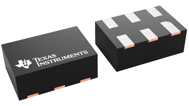
| Number of channels (#) | 1 |
| Total supply voltage (Max) (+5V=5, +/-5V=10) | 5.5 |
| Total supply voltage (Min) (+5V=5, +/-5V=10) | 2.7 |
| Rail-to-rail | In to V-, Out |
| GBW (Typ) (MHz) | 23 |
| Slew rate (Typ) (V/us) | 12 |
| Vos (offset voltage @ 25 C) (Max) (mV) | 1 |
| Iq per channel (Typ) (mA) | 1.65 |
| Vn at 1 kHz (Typ) (nV/rtHz) | 9 |
| Rating | Catalog |
| Operating temperature range (C) | -40 to 125 |
| Offset drift (Typ) (uV/C) | 0.7 |
| Features | EMI Hardened, Shutdown, Small Size |
| Input bias current (Max) (pA) | 10 |
| CMRR (Typ) (dB) | 94 |
| Output current (Typ) (mA) | 110 |
| Architecture | CMOS |
- Unless Otherwise Noted, Typical Values at TA = 25°C, V+ = 3.3V
- Supply Voltage 2.7V to 5.5V
- Supply Current 1.65 mA
- Shutdown Current 200 pA
- Input Offset Voltage 1 mV Max
- Input Bias Current 0.1 pA
- GBW 23 MHz
- EMIRR at 1.8 GHz 105 dB
- Input Noise Voltage at 1 kHz 9 nV/√Hz
- Slew Rate 12 V/μs
- Output Voltage Swing Rail-to-Rail
- Output Current Drive 70 mA
- Operating Ambient Temperature Range ?40°C to 125°C
- Space Saving Micro-UQFN Package 1.5 x 1.0 x 0.5 mm
All trademarks are the property of their respective owners.
The LMV881 is a low power CMOS input operational amplifier that provides low input bias currents, a rail to rail output with high output drive capability and a wide temperature range of ?40°C to +125°C. Additionally, the LMV881 is EMI hardened to minimize sensitivity to external interference.
The LMV881 has a maximum input offset voltage of 1 mV with an input common-mode voltage range that includes ground. Over an operating supply range from 2.7V to 5.5V, the LMV881 provides a typical PSRR of 110dB and a CMRR of 110dB. This makes the LMV881 ideal for EMI sensitive applications as well as exceptional performance as a robust general purpose part.
The unity gain stable LMV881 features 23 MHz of bandwidth while consuming only 1.65 mA of current. This device also maintains stability for capacitive loads as large as 200 pF.
LMV881 offers a shutdown pin that can be used to disable the device and reduce the supply current to sub-nanoamp levels. During shutdown, the output is hard-clamped to V- to provide a known output state. The shutdown input thresholds are set for 1.8V logic, regardless of the amplifiers supply voltage. This eliminates the need for additional logic level shifting circuitry or translators.
The LMV881 is offered in the space saving 6-Pin μUQFN package and provides excellent performance and economy in terms of power and space usage.