| Regulated outputs (#) | 13 |
| Vin (Min) (V) | 5.6 |
| Vin (Max) (V) | 21 |
| Iout (Max) (A) | 21, 25 |
| Rating | Catalog |
| LDO | 4 |
| Iq (Typ) (mA) | 0.3 |
| Features | Comm Control, Dynamic Voltage Scaling, Enable, Enable Pin, I2C Control, Over Current Protection, Power Good, Power Sequencing, Synchronous Rectification, Thermal Shutdown, UVLO Fixed |
| Processor name | Zynq Ultrascale+, Artix-7 |
| Processor supplier | Xilinx |
| Shutdown current (ISD) (Typ) (uA) | 65 |
| Switching frequency (Typ) (kHz) | 2500 |
| Configurability | Factory programmable, Software configurable |
- Wide VIN Range From 5.6V to 21 V
- Three Variable-Output Voltage Synchronous
Step-Down Controllers With DCAP2? Topology- Scalable Output Current Using External FETs
With Selectable Current Limit - I2C DVS Control From 0.41 V to 1.67 V in
10-mV Steps or 1 V to 3.575 V in 25-mV Steps
- Scalable Output Current Using External FETs
- Three Variable-Output Voltage Synchronous Step-Down
Converters With DCS-Control Topology- VIN Range From 4.5 V to 5.5 V
- Up to 3 A of Output Current
- I2C DVS Control From 0.41 V to 1.67 V
in 10-mV Steps or 0.425 V to 3.575 V in 25-mV
Steps
- Three LDO Regulators With Adjustable Output Voltage
- LDOA1: I2C-Selectable Output Voltage
From 1.35 V to 3.3 V for up to 200 mA of Output
Current - LDOA2 and LDOA3: I2C-Selectable Output
Voltage From 0.7 V to 1.5 V for up to 600 mA of
Output Current
- LDOA1: I2C-Selectable Output Voltage
- VTT LDO for DDR Memory Termination
- Three Load Switches With Slew Rate Control
- Up to 300 mA of Output Current With Voltage
Drop Less Than 1.5% of Nominal Input Voltage - RDSON < 96 mΩ at Input Voltage
of 1.8 V
- Up to 300 mA of Output Current With Voltage
- 5-V Fixed-Output Voltage LDO (LDO5)
- Power Supply for Gate Drivers of SMPS and
for LDOA1 - Automatic Switch to External 5-V Buck for Higher
Efficiency
- Power Supply for Gate Drivers of SMPS and
- Built-in Flexibility and Configurability by Factory
OTP Programming- Six GPI Pins Configurable to Enable (CTL1 to CTL6)
or Sleep Mode Entry (CTL3 and CTL6) of Any Selected
Rails - Four GPO Pins Configurable to Power Good of Any
Selected Rails - Open-Drain Interrupt Output Pin
- Six GPI Pins Configurable to Enable (CTL1 to CTL6)
- I2C Interface Supports:
- Standard Mode (100 kHz)
- Fast Mode (400 kHz)
- Fast Mode Plus (1 MHz)
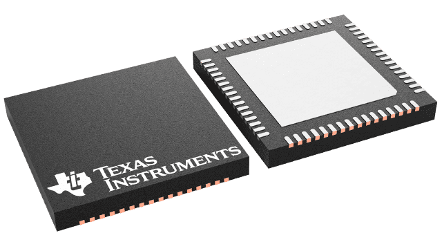
The TPS650860 device is a single-chip power-management IC designed for multicore processors, FPGAs, and other System-on-Chips (SoCs). The TPS650860 offers an input range of 5.6 V to 21 V, enabling a wide range of applications. The device is well suited for NVDC and non-NVDC power architecture using 2S, 3S, or 4S Li-Ion battery packs. See the Application Section for 5-V input supplies. The D-CAP2 and DCS-Control high-frequency voltage regulators use small inductors and capacitors to achieve a small solution size. The D-CAP2 and DCS-Control topologies have excellent transient response performance, which is great for processor core and system memory rails that have fast load switching. An I2C interface allows simple control either by an embedded controller (EC) or by an SoC. The PMIC comes in an 8-mm × 8-mm, single-row VQFN package with thermal pad for good thermal dissipation and ease of board routing.


