| Sample rate (Max) (MSPS) | 42 |
| Resolution (Bits) | 8 |
| Number of input channels | 1 |
| Interface type | Parallel CMOS |
| Analog input BW (MHz) | 120 |
| Features | Low Power |
| Rating | Catalog |
| Input range (Vp-p) | 0.73 |
| Power consumption (Typ) (mW) | 40 |
| Architecture | Pipeline |
| SNR (dB) | 45 |
| ENOB (Bits) | 7.2 |
| SFDR (dB) | 57 |
| Operating temperature range (C) | -40 to 85 |
| Input buffer | No |
- Low Input Capacitance
- Internal Sample-and-Hold Function
- Single +3V Operation
- Power Down Feature
- TRI-STATE Outputs
Key Specifications
- Resolution: 8 Bits
- Maximum Sampling Frequency: 42MSPS (min)
- ENOB @ fCLK = 42 MHz,
fIN = 4.4 MHz: 7.2 Bits (typ) - Ensured No Missing Codes
- Power Consumption: 40 mW (typ); 48 mW (max) (Excluding Reference Current)
The ADC08351 is an easy to use low power, low cost, small size, 42 MSPS analog-to-digital converter that digitizes signals to 8 bits. The ADC08351 uses an unique architecture that achieves 7.2 Effective Bits with a 4.4 MHz input and 42 MHz clock frequency and 6.8 Effective Bits with a 21 MHz input and 42 MHz clock frequency. Output formatting is straight binary coding.
To minimize system cost and power consumption, the ADC08351 requires minimal external components and includes input biasing to allow optional a.c. input signal coupling. The user need only provide a +3V supply and a clock. Many applications require no separate reference or driver components.
The excellent dc and ac characteristics of this device, together with its low power consumption and +3V single supply operation, make it ideally suited for many video and imaging applications, including use in portable equipment. Total power consumption is reduced to less than 7 mW in the power-down mode. Furthermore, the ADC08351 is resistant to latch-up and the outputs are short-circuit proof.
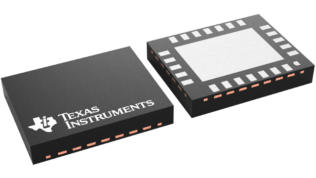
Fabricated on a 0.35 micron CMOS process, the ADC08351 is offered in TSSOP and WQFN (a molded lead frame-based chip-scale package), and is designed to operate over the industrial temperature range of ?40°C to +85°C.


