完善资料让更多小伙伴认识你,还能领取20积分哦,立即完善>
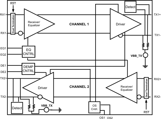
The SN65LVPE501 is a dual channel, single lane PCIe redriver and signal conditioner supporting data rates of up to 5.0Gbps. The device complies with PCIe spec revision 2.1.
Programmable EQ, De-Emphasis and Amplitude Swing
The SN65LVPE501 is designed to minimize the signal degradation effects such as crosstalk and inter-symbol interference (ISI) that limits the interconnect distance between two devices. The input stage of each channel offers selectable equalization settings that can be programmed to match loss in the channel. The differential outputs provide selectable de-emphasis to compensate for the anticipated distortion PCIe signal will experience. Level of de-emphasis will depend on the length of interconnect and its characteristics. Both equalization and de-emphasis levels are controlled by the setting of signal control pins EQ1, EQ2 and DE1, DE2.
To provide additional control of signal integrity in extended backplane applications LVPE501 provides independent output amplitude control for each channel. See for setting details.
Device PowerOn
Device initiates internal power-on reset after VCC has stabilized. External reset can also be applied at anytime by toggling RST pin. External reset is recommended after every device power-up. When RST is driven high, the device samples the state of EN_RXD, if it is set H device enters Rx.Detect state where each channel will perform Rx.Detect function (as described in PCIe spec). If EN_RXD is set L, automatic RX detect function is disabled and both channels are enabled with their termination set to ZDC_RX.
Receiver Detection
While EN_RXD pin is H and device is not in sleep mode (RST is H), SN65LVPE501 performs RX.Detect on both channels indefinitely until remote termination is detected on both channels. Automatic Rx detection feature can be forced off by driving EN_RXD low. In this state both channels input termination are set to ZDC_RX.
Sleep (Shut_Down) Mode
This is low power state triggered by RST = L. In sleep mode receiver termination resistor for each of the two channels is switched to ZRX-HIGH_IMP of >50 KΩ and transmitters are pulled to Hi-Z state. Device power is reduced to <1mW (TYP). To get device out of sleep mode RST is toggled L-H.
Electrical Idle Support
A link is in an electrical idle state when the TX± voltage is held at a steady constant value like the common mode voltage. SN65LVPE501 detects an electrical idle state when RX± input voltage of the associated channel falls below VEID_TH min. After detection of an electrical idle state in a given channel the device asserts electrical idle state in its corresponding TX. When RX± voltage exceeds VEID_TH max, normal device operation is restored and output starts passing input signal. Electrical idle exit and entry time is specified at ≤6ns.
Electrical idle support is independent for each channel.
Power Save Features
The device supports three power save modes as described below.
1. Sleep (Shut_Down) Mode
This mode can be enabled from any state (Rx detect or active) by driving RST L. In this state both channels have their termination set to ZRX-HIGH_IMP+ and outputs are at Hi-Z. Device power is 1mW (MAX)
2. Auto Low Power Mode
This mode is enabled when PS pin is tied H and device is in active mode. In this mode anytime Vindiff_pp falls below selected VEID_TH for a and stays below VEID_TH for >1µs (TYP), the associated CH will enter auto low power (ALP) mode where power/CH will be reduced to <1/3rd of normal operating power/CH or about 70mW under typical voltage of 3.3V when ALP conditions are met for both channels. A CH will exit ALP mode whenever Vindiff_pp exceeds max VEID_TH for that channel. Exit latency is 30ns max. To use this mode link latency will need to account for the ALP exit time for N_FTS. ALP mode is handled by each channel independently based on its input differential signal level. This mode can be disabled by leaving PS as NC or tying PS to GND via 4.7kύ.
3. Cable Disconnect Mode
This mode is activated when RST is H, EN_RXD = H, and no termination is detected by either channel. Device is in the Rx.Detect state whereby it is continuously performing Rx.Detect on both channels. In this state total power consumed by device is typically <3% of normal active power. Or <10mW (MAX).
Beacon Support
With its broadband design, the SN65LVPE501 supports low frequency Beacon signal (as defined by PCIe 2.1 spec) used to indicate wake-up event to the system by a downstream device when in L2 power state. All requirements for a beacon signal as specified in PCI Express specification 2.1 must be met for device to pass beacon signals.
Devic Power
The SN65LVPE501 is designed to operate from a single 3.3V supply. Always practice proper supply sequencing procedure. Apply VCC first before any input control pin signals are applied to the device. Power-down sequence is in reverse order.
| Device Type |
| Number of Channels (#) |
| Application |
| IN SigCon |
| OUT SigCon |
| Input Compatibility |
| Output Compatibility |
| Speed (Max) (Gbps) |
| SupplyVoltage (Volt) |
| Protocols |
| Operating Temperature Range (C) |
| Package Group |
| Pin/Package |
| SN65LVPE501 | SN65LVPE504 |
|---|---|
| Redriver | Redriver |
| 2 | 4 |
| USB3.0 & PCI Express GenII | USB3.0 & PCI Express GenII |
| EQ | EQ |
| DE | DE |
| AC-Coupled CML | AC-Coupled CML |
| AC-Coupled CML | AC-Coupled CML |
| 5 Gbps | 5 Gbps |
| 3.3 | 3.3 |
| PCIe | PCIe |
| -40 to 85 | -40 to 85 |
| VQFN | WQFN |
| 24VQFN | 42WQFN |
关注我们的微信

下载发烧友APP

电子发烧友观察

版权所有 © 湖南华秋数字科技有限公司
电子发烧友 (电路图) 湘公网安备43011202000918 电信与信息服务业务经营许可证:合字B2-20210191 工商网监
湘ICP备 2023018690 号
工商网监
湘ICP备 2023018690 号