0
  • 聊天消息
  • 系统消息
  • 评论与回复
登录后你可以
  • 下载海量资料
  • 学习在线课程
  • 观看技术视频
  • 写文章/发帖/加入社区
创作中心

完善资料让更多小伙伴认识你,还能领取20积分哦,立即完善>

3天内不再提示

TMS320C6747 定点/浮点数字信号处理器

数据:

描述

TMS320C6745 /6747器件是一款基于TMS320C674x DSP内核的低功耗数字信号处理器。它的功耗显着低于TMS320C6000 DSP平台的其他成员。

TMS320C6745 /6747器件使原始设备制造商(OEM)和原始设计制造商(ODM)能够快速推出市场上的设备。高处理性能。

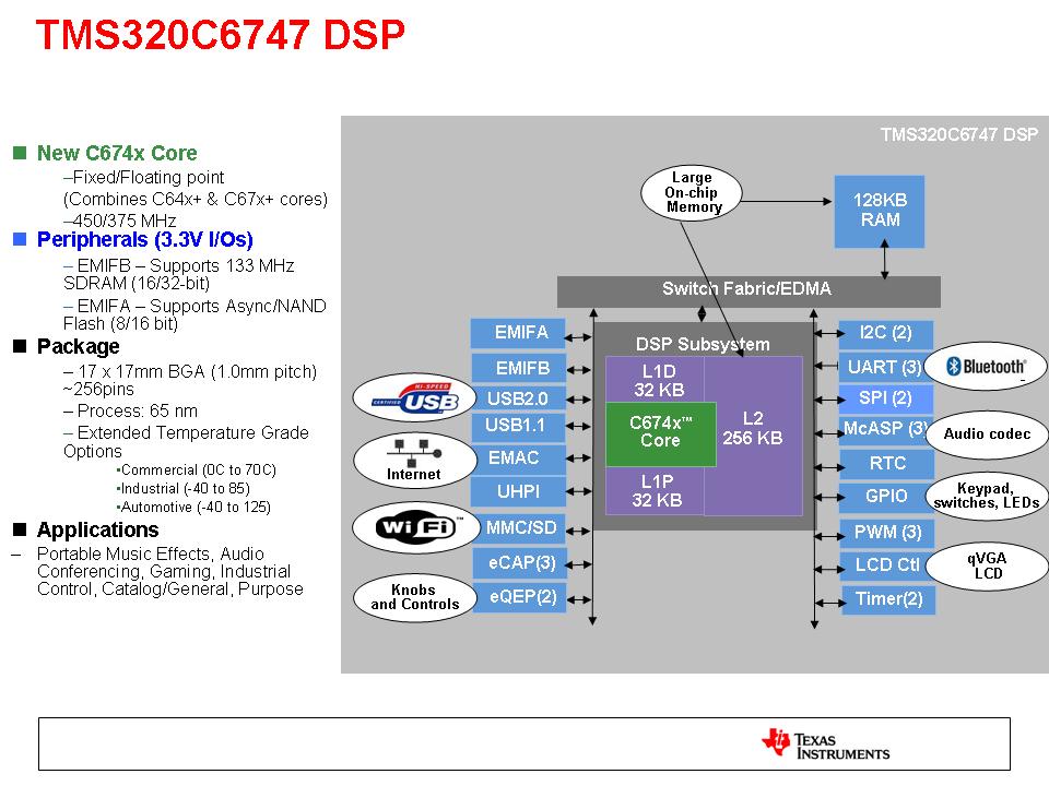
TMS320C6745 /6747 DSP内核采用基于缓存的两级架构。 1级程序高速缓存(L1P)是32 KB直接映射高速缓存,1级数据高速缓存(L1D)是32 KB双向组关联高速缓存。 2级程序高速缓存(L2P)由256 KB内存空间组成,在程序和数据空间之间共享。 L2内存可以配置为映射内存,缓存或两者的组合。虽然系统中的其他主机可以访问DSP L2,但是其他主机可以使用额外的128KB RAM共享内存(仅限TMS320C6747),而不会影响DSP性能。

外设集包括:带管理数据输入/输出(MDIO)模块的10/100 Mbps以太网MAC(EMAC);两个I 2 C总线接口; 3个多通道音频串行端口(McASP),带有16/9串行器和FIFO缓冲器;两个64位通用定时器,每个都可配置(一个可配置为看门狗);可配置的16位主机端口接口(HPI)[仅限TMS320C6747];多达8个16引脚的通用输入/输出(GPIO),具有可编程中断/事件生成模式,与其他外设复用; 3个UART接口(一个具有 RTS CTS );三个增强型高分辨率脉冲宽度调制器(eHRPWM)外设;三个32位增强型捕获(eCAP)模块外设,可配置为3个捕获输入或3个辅助脉冲宽度调制器(APWM)输出;两个32位增强型正交编码脉冲(eQEP)外设;和2个外部存储器接口:用于较慢存储器或外设的异步和SDRAM外部存储器接口(EMIFA),以及用于SDRAM的高速存储器接口(EMIFB)。

以太网媒体访问控制器(EMAC)提供TMS320C6745 /6747器件与网络之间的高效接口。 EMAC支持10Base-T和100Base-TX,或半双工或全双工模式下的10 Mbps和100 Mbps。此外,MDIO接口可用于PHY配置。

丰富的外设集可以控制外部外围设备并与外部处理器通信。有关每个外围设备的详细信息,请参阅本文档后面的相关章节以及相关的外围设备参考指南。

特性

  • Software Support
    • TI DSP/BIOS
    • Chip Support Library and DSP Library
  • 375- and 456-MHz TMS320C674x VLIW DSP
  • C674x Instruction Set Features
    • Superset of the C67x+ and C64x+ ISAs
    • Up to 3648 MIPS and 2736 MFLOPS C674x
    • Byte-Addressable (8-, 16-, 32-, and 64-Bit Data)
    • 8-Bit Overflow Protection
    • Bit-Field Extract, Set, Clear
    • Normalization, Saturation, Bit-Counting
    • Compact 16-Bit Instructions
  • C674x Two-Level Cache Memory Architecture
    • 32KB of L1P Program RAM/Cache
    • 32KB of L1D Data RAM/Cache
    • 256KB of L2 Unified Mapped RAM/Cache
    • Flexible RAM/Cache Partition (L1 and L2)
  • Enhanced Direct Memory Access Controller 3 (EDMA3):
    • 2 Transfer Controllers
    • 32 Independent DMA Channels
    • 8 Quick DMA Channels
    • Programmable Transfer Burst Size
  • TMS320C674x Fixed- and Floating-Point VLIW DSP Core
    • Load-Store Architecture with Nonaligned Support
    • 64 General-Purpose Registers (32-Bit)
    • Six ALU (32- and 40-Bit) Functional Units
      • Supports 32-Bit Integer, SP (IEEE Single Precision/32-Bit) and DP (IEEE Double Precision/64-Bit) Floating Point
      • Supports up to Four SP Additions Per Clock, Four DP Additions Every 2 Clocks
      • Supports up to Two Floating-Point (SP or DP) Reciprocal Approximation (RCPxP) and Square-Root Reciprocal Approximation (RSQRxP) Operations Per Cycle
    • Two Multiply Functional Units
      • Mixed-Precision IEEE Floating Point Multiply Supported up to:
        • 2 SP x SP -> SP Per Clock
        • 2 SP x SP -> DP Every Two Clocks
        • 2 SP x DP -> DP Every Three Clocks
        • 2 DP x DP -> DP Every Four Clocks
      • Fixed-Point Multiply Supports Two 32 x 32-Bit Multiplies, Four 16 x 16-Bit Multiplies, or Eight 8 x 8-Bit Multiplies per Clock Cycle, and Complex Multiples
    • Instruction Packing Reduces Code Size
    • All Instructions Conditional
    • Hardware Support for Modulo Loop
      Operation
    • Protected Mode Operation
    • Exceptions Support for Error Detection and Program Redirection
  • 128KB of RAM Shared Memory (TMS320C6747 Only)
  • 3.3-V LVCMOS I/Os (Except for USB Interfaces)
  • Two External Memory Interfaces:
    • EMIFA
      • NOR (8- or 16-Bit-Wide Data)
      • NAND (8- or 16-Bit-Wide Data)
      • 16-Bit SDRAM with 128-MB Address Space (TMS320C6747 Only)
    • EMIFB
      • 32-Bit or 16-Bit SDRAM with 256-MB Address Space (TMS320C6747)
      • 16-Bit SDRAM with 128-MB Address Space (TMS320C6745)
  • Three Configurable 16550-Type UART Modules:
    • UART0 with Modem Control Signals
    • Autoflow Control Signals (CTS, RTS) on UART0 Only
    • 16-Byte FIFO
    • 16x or 13x Oversampling Option
  • LCD Controller (TMS320C6747 Only)
  • Two Serial Peripheral Interfaces (SPIs) Each with One Chip Select
  • Multimedia Card (MMC)/Secure Digital (SD) Card Interface with Secure Data I/O (SDIO)
  • Two Master and Slave Inter-Integrated Circuit (I2C Bus™)
  • One Host-Port Interface (HPI) with 16-Bit-Wide Muxed Address/Data Bus for High Bandwidth (TMS320C6747 Only)
  • Programmable Real-Time Unit Subsystem (PRUSS)
    • Two Independent Programmable Realtime Unit (PRU) Cores
      • 32-Bit Load and Store RISC Architecture
      • 4KB of Instruction RAM per Core
      • 512 Bytes of Data RAM per Core
      • PRUSS can be Disabled via Software to Save Power
    • Standard Power-Management Mechanism
      • Clock Gating
      • Entire Subsystem Under a Single PSC Clock Gating Domain
    • Dedicated Interrupt Controller
    • Dedicated Switched Central Resource
  • USB 1.1 OHCI (Host) with Integrated PHY (USB1) (TMS320C6747 Only)
  • USB 2.0 OTG Port with Integrated PHY (USB0)
    • USB 2.0 High- and Full-Speed Client (TMS320C6747)
    • USB 2.0 Full-Speed Client (TMS320C6745)
    • USB 2.0 High-, Full-, and Low-Speed Host (TMS320C6747)
    • USB 2.0 Full- and Low-Speed Host (TMS320C6745)
    • High-Speed Functionality Available on TMS320C6747 Device Only
    • End Point 0 (Control)
    • End Points 1,2,3,4 (Control, Bulk, Interrupt or ISOC) RX and TX
  • Three Multichannel Audio Serial Ports (McASPs):
    • TMS320C6747 Supports 3 McASPs
    • TMS320C6745 Supports 2 McASPs
    • Six Clock Zones and 28 Serial Data Pins
    • Supports TDM, I2S, and Similar Formats
    • DIT-Capable (McASP2)
    • FIFO Buffers for Transmit and Receive
  • 10/100 Mbps Ethernet MAC (EMAC):
    • IEEE 802.3 Compliant (3.3-V I/O Only)
    • RMII Media-Independent Interface
    • Management Data I/O (MDIO) Module
  • Real-Time Clock with 32-kHz Oscillator and Separate Power Rail (TMS320C6747 Only)
  • One 64-Bit General-Purpose Timer (Configurable as Two 32-Bit Timers)
  • One 64-Bit General-Purpose Watchdog Timer (Configurable as Two 32-Bit General-Purpose Timers)
  • Three Enhanced Pulse Width Modulators (eHRPWMs):
    • Dedicated 16-Bit Time-Base Counter with Period and Frequency Control
    • 6 Single Edge, 6 Dual Edge Symmetric, or 3 Dual Edge Asymmetric Outputs
    • Dead-Band Generation
    • PWM Chopping by High-Frequency Carrier
    • Trip Zone Input
  • Three 32-Bit Enhanced Capture (eCAP) Modules:
    • Configurable as 3 Capture Inputs or 3 Auxiliary Pulse Width Modulator (APWM) Outputs
    • Single-Shot Capture of up to Four Event Time-Stamps
  • Two 32-Bit Enhanced Quadrature Encoder Pulse (eQEP) Modules
  • TMS320C6747 Device:
    • 256-Ball Pb-Free Plastic Ball Grid Array (PBGA) [ZKB Suffix], 1.0-mm Ball Pitch
  • TMS320C6745 Device:
    • 176-pin PowerPAD Plastic Quad Flat Pack [PTP suffix], 0.5-mm Pin Pitch
  • Commercial, Industrial, Extended, or Automotive Temperature

参数 与其它产品相比 C674x DSP

 
Operating Systems
DSP MHz (Max)
Display Options
DRAM
USB
EMAC
SATA
SPI
I2C
UART (SCI)
On-Chip L2 Cache/RAM
Other On-Chip Memory
Approx. Price (US$)
Applications
DSP
TMS320C6747 TMS320C6745
SYS/BIOS     TI RTOS    
375
456    
375
456    
1     0    
SDRAM     SDRAM    
2     1    
10/100     10/100    
0     2    
2     2    
2     2    
3     3    
256 KB     256 KB    
128 KB     0    
11.73 | 1ku     10.17 | 1ku    
Communications and Telecom
Consumer Electronics
Industrial    
Communications and Telecom
Consumer Electronics
Energy
Industrial
Medical    
1 C674x     1 C674x    

方框图 (1)


技术文档

数据手册(1)
元器件购买 TMS320C6747 相关库存