0
  • 聊天消息
  • 系统消息
  • 评论与回复
登录后你可以
  • 下载海量资料
  • 学习在线课程
  • 观看技术视频
  • 写文章/发帖/加入社区
创作中心

完善资料让更多小伙伴认识你,还能领取20积分哦,立即完善>

3天内不再提示

AM1806 Sitara 处理器

数据:

描述

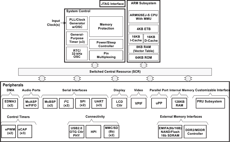
AM1806 ARM微处理器是基于ARM926EJ-S的低功耗应用处理器。

该设备使原始设备制造商( OEM(原始设计制造商)和原始设计制造商(ODM)通过完全集成的混合处理器解决方案的最大灵活性,快速向市场推出具有强大操作系统支持,丰富用户界面和高处理性能寿命的设备。

ARM926EJ-S是一个32位RISC处理器内核,可执行32位或16位指令并处理32位,16位或8位数据。核心使用流水线操作,以便处理器和内存系统的所有部分可以连续运行。

ARM内核具有协处理器15(CP15),保护模块以及数据和程序存储器管理单元(MMU)表后备缓冲区。 ARM核心处理器具有单独的16 KB指令和16 KB数据高速缓存。两者都是与虚拟索引虚拟标记(VIVT)的四向关联。 ARM内核还有8KB的RAM(矢量表)和64KB的ROM。

外设集包括:一个USB2.0 OTG接口;两个内部集成电路(I 2 C Bus)接口;一个多通道音频串行端口(McASP),带有16个串行器和FIFO缓冲器;两个带有FIFO缓冲器的多通道缓冲串行端口(McBSP);两个串行外设接口(SPI),具有多个芯片选择;四个64位通用定时器,每个都可配置(一个可配置为看门狗);可配置的16位主机端口接口(HPI);多达9组通用输入/输出(GPIO)引脚,每个引脚包含16个引脚,具有可编程中断和事件生成模式,与其他外设复用;三个UART接口(每个接口都有 RTS CTS );两个增强型高分辨率脉冲宽度调制器(eHRPWM)外设;三个32位增强型捕获(eCAP)模块外设,可配置为3个捕获输入或3个辅助脉冲宽度调制器(APWM)输出;两个外部存储器接口;用于较慢存储器或外设的异步和SDRAM外部存储器接口(EMIFA);

通用并行端口(uPP)为许多类型的数据转换器,FPGA或其他并行设备提供高速接口。 uPP支持两个通道上8到16位的可编程数据宽度。支持单数据速率和双数据速率传输以及START,ENABLE和WAIT信号,以便为各种数据转换器提供控制。

包含视频端口接口(VPIF),提供灵活的视频I /O端口。

丰富的外设集可以控制外部外围设备并与外部处理器通信。有关每个外设的详细信息,请参阅本文档中的相关章节以及相关的外设参考指南。

该器件具有一整套用于ARM处理器的开发工具。这些工具包括C编译器和调度,以及用于查看源代码执行情况的Windows调试器界面。

特性

  • 375- and 456-MHz ARM926EJ-S RISC MPU
  • Enhanced Direct Memory Access Controller 3 (EDMA3):
    • 2 Channel Controllers
    • 3 Transfer Controllers
    • 64 Independent DMA Channels
    • 16 Quick DMA Channels
    • Programmable Transfer Burst Size
  • 1.8-V or 3.3-V LVCMOS I/Os (Except for USB and DDR2 Interfaces)
  • Two External Memory Interfaces:
    • EMIFA
      • NOR (8- or 16-Bit-Wide Data)
      • NAND (8- or 16-Bit-Wide Data)
      • 16-Bit SDRAM with 128-MB Address Space
    • DDR2/Mobile DDR Memory Controller with one of the following:
      • 16-Bit DDR2 SDRAM with 256-MB Address Space
      • 16-Bit mDDR SDRAM with 256-MB Address Space
  • Three Configurable 16550-Type UART Modules:
    • With Modem Control Signals
    • 16-Byte FIFO
    • 16x or 13x Oversampling Option
  • LCD Controller
  • Two Serial Peripheral Interfaces (SPIs) Each with Multiple Chip Selects
  • Two Multimedia Card (MMC)/Secure Digital (SD) Card Interfaces with Secure Data I/O (SDIO) Interfaces
  • Two Master and Slave Inter-Integrated Circuits
    (I2C Bus)
  • One Host-Port Interface (HPI) with 16-Bit-Wide Muxed Address and Data Bus For High Bandwidth
  • Programmable Real-Time Unit Subsystem (PRUSS)
    • Two Independent Programmable Real-Time Unit (PRU) Cores
      • 32-Bit Load-Store RISC Architecture
      • 4KB of Instruction RAM per Core
      • 512 Bytes of Data RAM per Core
      • PRUSS can be Disabled via Software to Save Power
      • Register 30 of Each PRU is Exported from the Subsystem in Addition to the Normal R31 Output of the PRU Cores.
    • Standard Power-Management Mechanism
      • Clock Gating
      • Entire Subsystem Under a Single PSC Clock Gating Domain
    • Dedicated Interrupt Controller
    • Dedicated Switched Central Resource
  • USB 2.0 OTG Port with Integrated PHY (USB0)
    • USB 2.0 High- and Full-Speed Client
    • USB 2.0 High-, Full-, and Low-Speed Host
    • End Point 0 (Control)
    • End Points 1,2,3,4 (Control, Bulk, Interrupt or ISOC) RX and TX
  • One Multichannel Audio Serial Port (McASP):
    • Transmit and Receive Clocks
    • Two Clock Zones and 16 Serial Data Pins
    • Supports TDM, I2S, and Similar Formats
    • DIT-Capable
    • FIFO Buffers for Transmit and Receive
  • Two Multichannel Buffered Serial Ports (McBSPs):
    • Transmit and Receive Clocks
    • Supports TDM, I2S, and Similar Formats
    • AC97 Audio Codec Interface
    • Telecom Interfaces (ST-Bus, H100)
    • 128-Channel TDM
    • FIFO Buffers for Transmit and Receive
  • Video Port Interface (VPIF):
    • Two 8-Bit SD (BT.656), Single 16-Bit or Single Raw (8-, 10-, and 12-Bit) Video Capture Channels
    • Two 8-Bit SD (BT.656), Single 16-Bit Video Display Channels
  • Universal Parallel Port (uPP):
    • High-Speed Parallel Interface to FPGAs and Data Converters
    • Data Width on Both Channels is 8- to 16-Bit Inclusive
    • Single-Data Rate or Dual-Data Rate Transfers
    • Supports Multiple Interfaces with START, ENABLE, and WAIT Controls
  • Real-Time Clock (RTC) with 32-kHz Oscillator and Separate Power Rail
  • Three 64-Bit General-Purpose Timers (Each Configurable as Two 32-Bit Timers)
  • One 64-Bit General-Purpose or Watchdog Timer (Configurable as Two 32-Bit General-Purpose Timers)
  • Two Enhanced High-Resolution Pulse Width Modulators (eHRPWMs):
    • Dedicated 16-Bit Time-Base Counter with Period and Frequency Control
    • 6 Single-Edge Outputs, 6 Dual-Edge Symmetric Outputs, or 3 Dual-Edge Asymmetric Outputs
    • Dead-Band Generation
    • PWM Chopping by High-Frequency Carrier
    • Trip Zone Input
  • Three 32-Bit Enhanced Capture (eCAP) Modules:
    • Configurable as 3 Capture Inputs or 3 Auxiliary Pulse Width Modulator (APWM) Outputs
    • Single-Shot Capture of up to Four Event Time-Stamps
  • 361-Ball Pb-Free Plastic Ball Grid Array (PBGA) [ZCE Suffix], 0.65-mm Ball Pitch
  • 361-Ball Pb-Free PBGA [ZWT Suffix], 0.80-mm Ball Pitch
  • Commercial or Extended Temperature

参数 与其它产品相比 AM1x

 
Arm MHz (Max.)
DRAM
Display
USB
EMAC
SPI
I2C
UART
Operating Temperature Range (C)
Approx. Price (US$)
AM1806 AM1802 AM1808 AM1810
375
456    
300     375
456    
375
456    
DDR2
LPDDR    
DDR2
LPDDR    
DDR2
LPDDR    
DDR2
LPDDR    
1 LCD       1 LCD     1 LCD    
1     1     1     1    
  10/100     10/100     10/100    
2     2     2     2    
2     1     2     2    
3     3     3     3    
-40 to 105
0 to 90
-40 to 90    
-40 to 90     0 to 90
-40 to 105
-40 to 90    
-40 to 105    
8.36 | 1ku     8.25 | 1ku     9.28 | 1ku     18.53 | 1ku    

方框图 (3)


技术文档

数据手册(1)
元器件购买 AM1806 相关库存

相关阅读