 STGAP2SCM电流隔离4A单个栅极驱动器解决方案
ST公司的STGAP2SCM是电流隔离1700V单个栅极驱动器,能隔离栅极驱动通路与低压控制电路和接口电路。驱动电流4A,并具有轨到轨输出,是得器件适合于大功率逆变器应用如工业应用中的马达驱动器。器件有两种不同的配置:单独输出引脚允许采用专用栅极电阻来单独优化开和关闭状态。其二,单输出引脚和米勒箝位功能在半桥拓扑中快速换向时避免出现栅极尖峰。两种配置具有高度灵活性,并大大降低了外接元件。器件集成的保护功能包括UVLO和热关断。而双输入引脚可选择控制信号的极性,同时可实现HW联锁保护,以避免控制器故障时所出现的交叉导通。输入到输出传输时延在80ns内,提供高PWM控制精度。栅极驱动电压高达26V,带延迟的3.3V,5V TTL/CMOS输入,主要用在家用电器,工厂自动化,工业驱动和风扇的马达驱动,600V/1200V逆变器,电池充电器,电感加热,焊接,UPS,电源单元,DC/DC转换器以及功率因素修正。本文介绍了STGAP2SCM主要特性,框图,多种应用电路以及评估板EVALSTGAP2SCM主要特性,电路图,材料清单和PCB设计图。
The STGAP2S is a single gate driver whichisolates the gate driving channel from the lowvoltage control and interface circuitry.
The gate driver is characterized by 4 A capabilityand rail-to-rail outputs, making the device alsosuitable for high power inverter applications suchas motor drivers in industrial applications.The device is available in two differentconfigurations. The configuration with separatedoutput pins allows to independently optimizeturnonand turn-off by using dedicated gate resistors.
A configuration featuring single output pin andMiller clamp function prevents gate spikes duringfast commutations in half-bridge topologies.
Both configurations provide high flexibility and billof material reduction for external components.The device integrates protection functions: UVLOand thermal shutdown are included to easilydesign high reliability systems. Dual input pinsallow choosing the control signal polarity and alsoimplementing HW interlocking protection in orderto avoid cross-conduction in case of controllermalfunction.
The input to output propagation delay resultscontained within 80 ns, providing high PWMcontrol accuracy.A standby mode is available in order to reduceidle power consumption.
STGAP2SCM主要特性:
1700 V single channel gate driver
Driver current capability: 4 A sink/sourceat 25℃
dV/dt transient immunity ± 100 V/ns
Overall input-output propagation delay: 80 ns
Separate sink and source for easy gate drivingconfiguration
4 A Miller clamp dedicated pin
UVLO function
Gate driving voltage up to 26 V
3.3 V, 5 V TTL/CMOS inputs with hysteresis
Temperature shutdown protection
Standby function
STGAP2SCM应用:
Motor driver for home appliances, factoryautomation, industrial drives and fans.
600/1200 V inverters
Battery chargers
Induction heating
Welding
UPS
Power supply units
DC-DC converters
Power factor correction
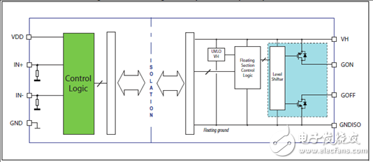
图1.STGAP2SCM框图-单独输出选择
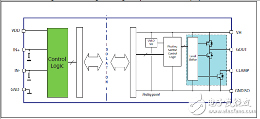
图2.STGAP2SCM框图-单独输出和米勒箝位选择
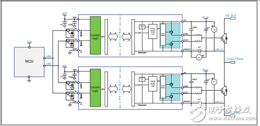
图3.STGAP2SCM单极和双极栅极驱动的电源配置图
图4.STGAP2SCM应用框图-单独输出
图5.STGAP2SCM应用框图-单独输出和负栅极驱动
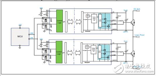
图6.STGAP2SCM应用框图-米勒箝位
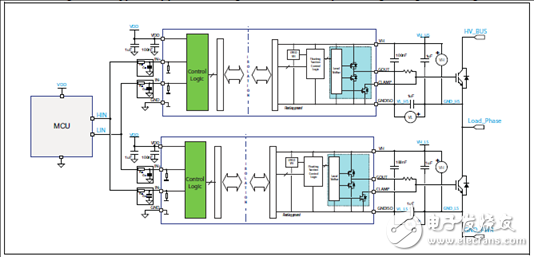
图6.STGAP2SCM应用框图-米勒箝位和负栅极驱动
评估板EVALSTGAP2SCM
STMicroelectronics EVALSTGAP2SCM Demonstration Board is used to evaluate the STGAP2SCM. The STGAP2SCM is an isolated single gate driver with a 4A current capability and rail-to-rail outputs. This makes the device ideal for high power inverter applications like motor drivers in industrial applications equipped with MOSFET/IGBT/SiC power switches. Two different variants are available: one with separated source and sink outputs, the other with single output pin and a dedicated pin for Miller clamp function. The EVALSTGAP2S is suitable for both output configuration variants.
The EVALSTGAP2S board allows evaluating allthe STGAP2SCM features while driving a halfbridgepower stage with voltage rating up to 1700V in TO-220 or TO-247 package.
The board facilitates the selection andmodification of the values of relevant externalcomponents in order to ease driver’s performanceevaluation under different applicative conditionsand fine pre-tuning of final applicationcomponents.
评估板EVALSTGAP2SCM主要特性:
High voltage rail up to 1700V
Driver current capability:
4A source/sink at 25℃
Separate sink and source for simplified gate driving configuration (STGAP2SM)
4A Miller clamp (STGAP2SCM)
Short propagation delay: 100ns
UVLO function
Gate driving voltage up to 26V
Negative gate driving
On-board isolated DC-DC converters to supply
gate drivers, fed by VAUX = 5V
VDD logic supply local 3.3V or VAUX
3.3V, 5V TTL/CMOS inputs with hysteresis
Easy jumper selection of driving voltage configuration:
+15/0V; +15/-3V; +19/0V; +19/-3V
Temperature shutdown protection
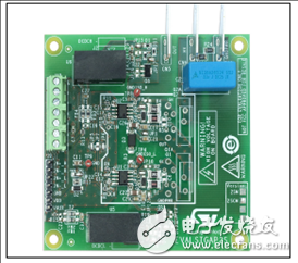
图7.评估板EVALSTGAP2SCM外形图
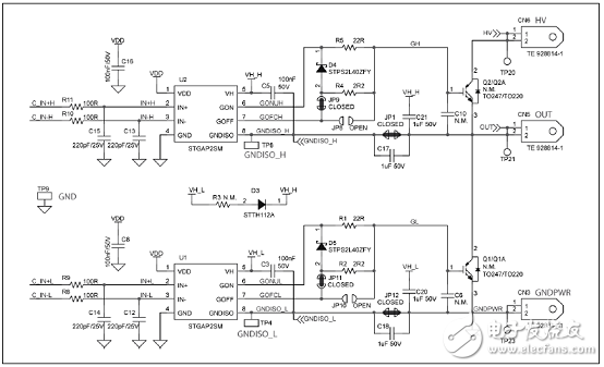
图8.评估板EVALSTGAP2SCM电路图(1):单独输出栅极驱动
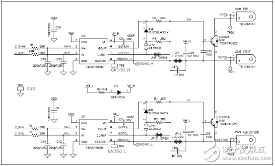
图9.评估板EVALSTGAP2SCM电路图(2):单独输出和米勒箝位的栅极驱动
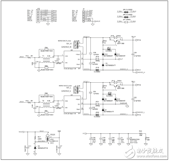
图10.评估板EVALSTGAP2SCM电路图(3):电源,连接器和去耦
评估板EVALSTGAP2SCM材料清单:
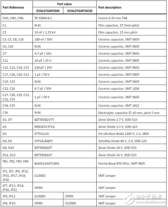
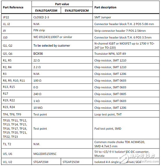
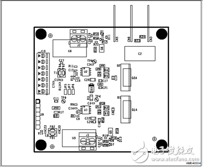
图11.评估板EVALSTGAP2SCM PCB设计图:顶层元件布放图
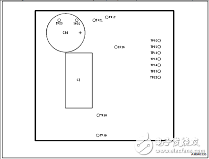
图12.评估板EVALSTGAP2SCM PCB设计图:底层元件布放图
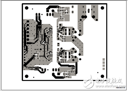
图13.评估板EVALSTGAP2SCM PCB设计图:顶层布局图
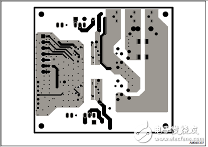
图14.评估板EVALSTGAP2SCM PCB设计图:底层布局图
详情请见:
https://www.st.com/content/ccc/resource/technical/layouts_and_diagrams/schematic_pack
/group0/a5/25/94/36/2f/d9/4a/9a/EVALSTGAP2SCM_SCHEMATICS/files/EVALSTGAP2SCM_SCHEMATICS.pdf
/jcr:content/translations/en.EVALSTGAP2SCM_SCHEMATICS.pdf
和https://www.st.com/content/ccc/resource/technical/document/bill_of_materials/group0/c8/7a
/24/ed/d7/f3/42/ed/EVALSTGAP2SCM_Bill_of_Material/files/EVALSTGAP2SCM_BOM.pdf/jcr:content
/translations/en.EVALSTGAP2SCM_BOM.pdf
en.EVALSTGAP2SCM_BOM.pdf
en.EVALSTGAP2SCM_SCHEMATICS.pdf
evalstgap2scm.pdf
-
栅极驱动器
+关注
关注
8文章
657浏览量
38597 -
电流隔离
+关注
关注
1文章
18浏览量
9818
发布评论请先 登录
相关推荐


 工商网监
工商网监
评论