 基于CYW20719的无线基带处理器解决方案
Cypress公司的CYW20719是兼容BT 5.0单独可用的基带处理器,集成了带BLE,EDR和BR的2.4GHz收发器;采用先进的40nm CMOS低功耗制造工艺,实现了高度集成以降低了外接元件,因此最小化应用占位面积和成本。器件支持自适应跳频(AFH),发送功率4dBm,接收灵敏度-95.5dBm(BLE),超低功耗无线电接收电流5.9mA(BLE),发送电流5.6mA@ 0 dBm(BLE),MCU子系统采用具有浮点单元(FPU)的96MHz Arm Cortex-M4 MCU,支持串行线调试(SWD),运行蓝牙堆栈和应用,集成了1MB闪存,512KB RAM和2MB ROM,存储了蓝牙堆栈和驱动器以及为用户应用的卸载闪存。主要用在可穿戴和健身,耳机和耳塞,家庭自动化,血压监测仪和其它医疗应用,接近传感器, 钥匙型控制终端, 恒温器和温度计以及玩具。本文介绍了CYW20719主要特性,功能框图,蓝牙无线模块CYBT-423028-02主要优势和功能特性,功能框图和电路图,评估板CYW920735Q60EVB-01 EVB主要特性,框图,概述图和主要元件分布,电路图和材料清单与PCB设计图。
The CYW20719 is a BT 5.0 compliant, stand-alone baseband processor with an integrated 2.4 GHz transceiver with BLE, EDR andBR. The device is intended for use in audio, IoT, sensors (medical, home, security, and so forth) and human interface device (HID)applications. Manufactured using an advanced 40nm CMOS low-power fabrication process, the CYW20719 employs high level ofintegration to reduce external components, thereby minimizing application footprint and costs.
This datasheet provides details of the functional, operational, and electrical characteristics of the CYW20719 device. It is intended forhardware, design, application, and OEM engineers.
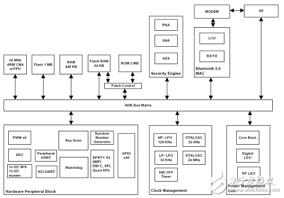
图1. CYW20719功能框图
CYW20719主要特性:
Bluetooth Subsystem
■ Complies with Bluetooth Core Specification v5.0 with LE 2Mbps
■ Supports Basic Rate (BR), Enhanced Data Rate (EDR) 2&3Mbps, Bluetooth Low Energy (BLE)
■ Supports Adaptive Frequency Hopping (AFH)
■ TX power 4 dBm
■ RX sensitivity -95.5 dBm (BLE)
■ Ultra-low-power radio
❐RX current 5.9 mA (BLE)
❐TX current 5.6 mA @ 0 dBm (BLE)
Coexistence Support
■ Support for Global Coexistence Interface for easy coexistenceimplementation with select Cypress Wi-Fi devices
MCU Subsystem
■ 96-MHz Arm Cortex-M4 microcontroller unit (MCU) with floatingpoint unit (FPU)
■ Supports serial wire debug (SWD)
■ Runs Bluetooth stack and application
■ Option to execute from on-chip flash or RAM
Memory Subsystem
■ 1 MB flash
■ 512 KB RAM
■ 2 MB ROM that stores Bluetooth stack and driver and offloadsflash for user applications
Audio features and interfaces
■ 1x I2S with master and slave modes
■ 1x PCM
■ PDM2
■ Analog front end for analog microphone1
Clocks
■ On-chip 32 kHz oscillator (LP-LPO)
■ On-chip 128 kHz oscillator (HP-LPO)
■ 32 kHz crystal oscillator (Optional if low power modes notrequired)
■ 24 MHz crystal oscillator
■ 48-bit real time clock (RTC)
Peripherals and communication
■ 6x 16-bit PWMs
■ Programmable key-scan matrix interface, up to 8x20 keyscanningmatrix 1,2
■ Quadrature decoder2
■ Watchdog timer (WDT)
■ 1x peripheral UART, 1x UART for programming and HCI
■ 2x SPI (master/slave mode) Blocks (SPI, Quad SPI, andMIPI DBI-C)
■ 1x I2C master/slave and 1x I2C master
■ 1x 28-channel ADC (10-ENOB for DC measurement and 12-ENOB for Audio measurement)
■ Hardware security engine2
General Purpose Input Output (GPIO)
■ 16 GPIOs on QFN package
■ 40 GPIOs on WLCSP package
■ Support up to 3.63 V operation
■ Four GPIOs support 16 mA and 8 mA sink at 3.3 V and 1.8 Vrespectively
Operating voltage and low-power support
■ Wide operating voltage range: 1.90 V to 3.63 V
■ 5 power modes to implement ultra-low power application –managed by real time operating system
■ 0.4 uA current in HID-OFF mode (wake from GPIO)。
Packages
■ 5 mm x 5 mm 40-pin quad flat no-lead (QFN)
■ 3.2 mm x 3.1 mm 134-ball Wafer Level Chip Scale Package(WLCSP)
Software Support
■ WICED Studio
CYW20719应用:
■ Wearables and Fitness bands
■ Headsets, earbuds, and other audio solutions
■ Home automation
■ Blood pressure monitors and other medical applications
■ Proximity sensors
■ Key Fobs
■ Thermostats and thermometers
■ Toys
The Bluetooth Baseband Core (BBC) implements all time-critical functions required for high-performance Bluetooth operation. TheBBC manages the buffering, segmentation, and routing of data for all connections. It prioritizes and schedules all RX/TX activitiesincluding adv, paging, scanning, and servicing of connections. In addition to these functions, it independently handles the hostcontroller interface (HCI) including all commands, events, and data flowing over HCI. The core also handles symbol timing, forwarderror correction (FEC), header error control (HEC), cyclic redundancy check (CRC), authentication, data encryption/decryption, anddata whitening/dewhitening.
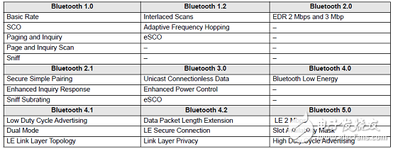
表1.蓝牙特性
蓝牙无线模块CYBT-423028-02
The CYBT-423028-02 is a dual-mode Bluetooth BR/EDR and Low Energy (BLE) wireless module solution. The CYBT-423028-02includes onboard crystal oscillators, passive components, and the Cypress CYW20719 silicon device.
The CYBT-423028-02 supports a number of peripheral functions (ADC, PWM), as well as multiple serial communication protocols(UART, SPI, I2C, I2S/PCM)。 The CYBT-423028-02 includes a royalty-free BLE stack compatible with Bluetooth 5.0 in a small 11.0 ×11.0 × 1.70mm module form-factor.
The CYBT-423028-02 includes an integrated chip antenna, is qualified by Bluetooth SIG, and includes regulatory certification approvalfor FCC, ISED, MIC, and CE.
蓝牙无线模块CYBT-423028-02功能特性:
■ 1x ADC with (10-bit ENoB for DC measurement and 12-bitENoB for Audio measurement) with 11 channels.
■ 1x HCI UART for programming and HCI
■ 1x peripheral UART (PUART)
■ 2x SPI (master or slave mode) blocks (SPI, Quad SPI, and MIPIDBI-C)
■ 1x I2C master/slave and 1x I2C master only
■ I2S/PCM audio interfaces
■ Up to six 16-bit PWMs
■ Watchdog Timer (WDT)
■ Bluetooth Basic Rate (BR) and Enhanced Data Rate (EDR)Support
■ BLE protocol stack supporting generic access profile (GAP)Central, Peripheral, or Broadcaster roles
■ Hardware Security Engine
蓝牙无线模块CYBT-423028-02主要优势:
CYBT-423028-02 is fully integrated and certified solution thatprovides all necessary components required to operateBluetooth communication standards.
■ Proven hardware design ready to use
■ Ultra-flexible supermux I/O designs allows maximum flexibilityfor GPIO function assignment
■ Large nonvolatile memory for complex application development
■ Over-the-Air (OTA) update capable for development or fieldupdates
■ Bluetooth SIG qualified with QDID and Declaration ID
■ WICED™ Studio provides an easy-to-use integrated designenvironment (IDE) to configure, develop, program, and testyour Bluetooth application
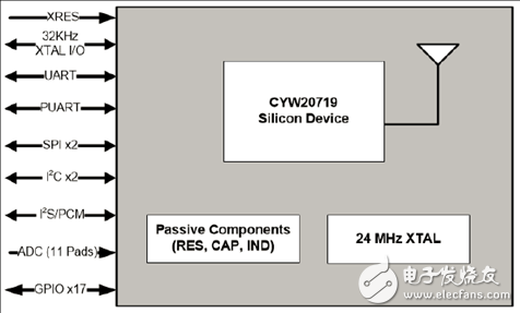
图2. 蓝牙无线模块CYBT-423028-02功能框图
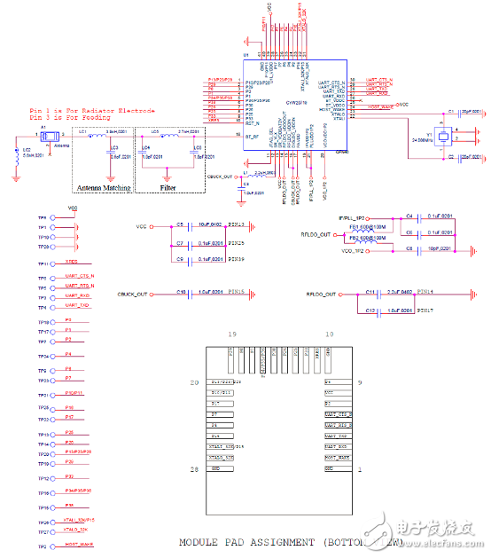
图3. 蓝牙无线模块CYBT-423028-02电路图
评估板CYW920735Q60EVB-01 EVB
Thank you for your interest in the CYW920735Q60EVB-01 Evaluation Board (EVB)。 The CYW920735Q60EVB-01 EVB enables customers to evaluate and develop single-chip Bluetooth and Bluetooth Low Energy (BLE) applications using the CYW20735B1, dual-mode Bluetooth 5.0 (BLE and BR) wireless MCU.
The CYW920735Q60EVB-01 EVB can be used with WICED™ Studio to develop and debug your CYW20735 project. The CYW920735Q60EVB-01 EVB offers footprint-compatibility with Arduino shields. In addition, the kit features an onboard programmer and USB-UART chip. The CYW920735Q60EVB-01 EVB supports 1.8 V and 3.3 V operation.
The CYW920735Q60EVB-01 EVB and CYW20735B1 device are supported in WICED Studio. The development system is compatible with Windows, OS X, and Linux operating systems. This document provides instructions for developing sample applications using WICED Studio.
图4.评估板CYW920735Q60EVB-01 EVB套件外形图
评估板CYW920735Q60EVB-01 EVB主要特性:
1. CYW20735B1-based carrier board with onboard antenna
2. Expansion headers that are compatible with Arduino shields
3. Support for 1.8 V and 3.3 V operation of the CYW20735 device
4. Two user-controlled LEDs, one push button, one recovery button, and one reset button
5. Onboard micro-USB connector for programming and debug purposes
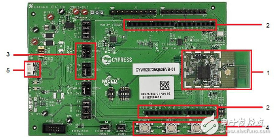
图5.评估板CYW920735Q60EVB-01 EVB外形图
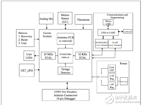
图6.评估板CYW920735Q60EVB-01 EVB框图
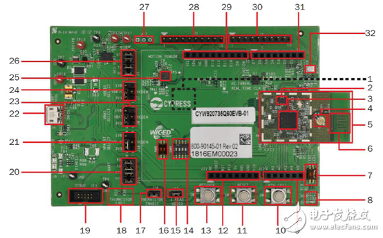
图7.评估板CYW920735Q60EVB-01 EVB概述图(正面)
图8.评估板CYW920735Q60EVB-01 EVB概述图(背面)
图7/8数字说明:
1. Coin Cell Holder (ZB1): This is a coin cell battery holder located on the bottom side of the development kit.
2. 8 Mb Serial Flash (U1): This is a SPI Flash of 8-Mbit to store applications and patch codes.
3. CYW20735(U1. U3): The Bluetooth (BR- Basic Rate) and Bluetooth Low Energy 5 qualified System-On-Chip from Cypress is the heart of this development kit. 4. External Antenna Connector (U1.J1): The external antenna connector is an RF connector fed from the BT_RF pad of the CYW20735 followed by a band pass filter. Please see Hardware design guidelines for more details.
5. Carrier Module (U1): The carrier module has the CYW20735 SoC on it. A Bluetooth antenna is etched on the carrier module PCB. The UART and GPIOs are brought out from the SoC pads to interface with the base board.
6. PCB Antenna (A1): The PCB antenna is the EM wave radiating part of the evaluation board which is fed from the BT_RF pad of the CYW20735 followed by a band pass filter and an Antenna matching circuit.
7. LED Enable Switch (SW4): These DIP switches are used to connect/disconnect the user controlled LEDs from the CYW20735 device.
8. LEDs (D1 and D2): These onboard LEDs can be controlled by the CYW20735 device. The LEDs are active LOW, so the pins must be driven to ground to turn ON the LEDs.
9. Arduino Header (J12): The Arduino-compatible I/O header brings out pins from CYW20735 to interface with Arduino shields.
10. User Button (SW3): This button can be used to provide an input to the CYW20735 device. Note that the button connects the CYW20735 pin to ground when pressed, so the CYW20735 pin must be configured as a digital input with resistive pull-up for detecting the button press.
11. Reset Button (SW2): This button can be used to reset the device.
12. Arduino Header (J11): The Arduino-compatible I/O header brings out pins from CYW20735 to interface with Arduino shields.
13. Recovery Button (SW1): This button is used to put the device in recovery mode. To put the device in recovery mode, press and hold the recovery button, press and release the reset button, then release the recovery button.
14. Recovery Button and Peripheral Power Switch (SW8): The DIP switch allows the user to disconnect the supply to onboard peripheral devices like motion sensor, thermistor, analog mic and real-time clock by disabling VDDP. It also allows configuration of the Recovery button connection. The recovery button connection should not be changed for this EVB – the other options are only used on other variants of the base board.
15. VDDIO Current Measurement Header (J15): This jumper is used to power the carrier board. To measure the current consumed by the carrier module, remove this jumper and connect an ammeter to the two pins.
16. SWD/GPIO Switch (SW9): This DIP switch allows the user to route the functionality of GPIO/SWD lines to either J4 Arduino Header or J13 debug header.
17. Thermistor Enable Header (J14): This jumper can be used to connect or disconnect the thermistor from the CYW20735 device.
18. Thermistor (R30): The onboard thermistor is a NTC analog thermistor that can be used to measure temperature.
19. Debug Header (J13): J13 is a 10-pin interface header that can be used to connect an external debugger via SWD.
20. PUART Header (J10): This header can be used to connect or disconnect the PUART pins from the USB-Serial device.
21. VPA_BT Select Header (J16): This header is used to select the VPA_BT (Power Amplifier supply) power source. The possible selections are 3.3 V, 1.8 V, or VCOIN which is the coin cell battery holder on the back of the board. Typically, VPA_BT should always be 3.3 V to get the maximum power levels mentioned in the datasheet.
22. USB Connector (J6): J6 is a micro USB female connector for connecting a USB cable to a PC.
23. VBAT Select Header (J8): This header is used to select the VBAT (Core power supply) power source. The possible selections are 3.3 V, 1.8 V, or VCOIN which is the coin cell battery holder on the bottom side of the board.
24. VDDIO Select Header (J7): This header is used to select the VDDIO power source. The possible selections are 3.3 V, 1.8 V, or VCOIN which is the coin cell battery holder on the bottom side of the board.
25. Motion Sensor (U2): This is an I2C-based 9-axis inertial module.
26. HCI UART Header (J5): This header can be used to connect or disconnect HCI UART from the USB-Serial device.
27. Motion Sensor Interrupt Test-point (J17): J17 has 3 test points for the interrupts from the motion sensor (U2)。
28. WICED Header (J1): This header brings out some pins of the CYW20735 device that are not connected to the Arduino headers. These pins can be used for testing or for custom applications.
29. Arduino Header (J3): The Arduino-compatible I/O header brings out pins from CYW20735 to interface with Arduino shields.
30. WICED Header (J2): This header brings out some pins of the CYW20735 device that are not connected to the Arduino headers. These pins can be used for testing or for custom applications.
31. Arduino Header (J4): The Arduino-compatible I/O header brings out pins from CYW20735 to interface with Arduino shields.
32. Analog Mic (MIC1): This is a MEMS microphone capable of recording voice which outputs to the micnand micppins of the CYW20735.
33. BT UART Voltage Level translator (U7): This voltage level translator IC allows interoperability of devices with different high-level voltage and low-level voltage for input and output operations.
34. USB to UART converter (U8): This is a two channel USB to serial UART IC for communicating between the CYW920735 and a PC.
35. EEPROM (U10): This EEPROM contains the configuration information for the USB to UART Converter for acting as USB Slave.
36. PUART Voltage Level translator (U9): This voltage level translator IC allows the interoperability of devices with different high-level voltage and low-level voltage for input and output operations.
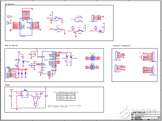
图9.评估板CYW920735Q60EVB-01 EVB电路图
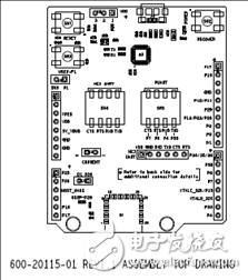
图10.评估板CYW920735Q60EVB-01 EVB PCB设计图(正面)
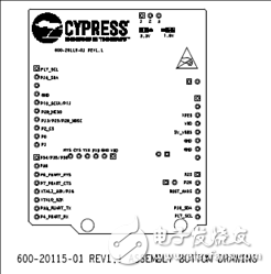
图11.评估板CYW920735Q60EVB-01 EVB PCB设计图(背面)
评估板CYW920735Q60EVB-01 EVB材料清单见:
CYBT-423028-EVAL BOM REV1.1_0
CYBT-423028-EVAL BOM REV1.1_0.xls
-
处理器
+关注
关注
68文章
18202浏览量
221927 -
基带
+关注
关注
4文章
156浏览量
30562
发布评论请先 登录
相关推荐


 工商网监
工商网监
评论