 ST STM32MP157C高性能低功耗MPU开发方案
ST公司的stm32MP157C是基于高性能双核ARM® Cortex®-A7 32位RISC核,工作频率高达650MHz,Cortex-A7处理器包括用于每个CPU的32KB L1指令缓存,32KB L1数据缓存以及256KB L2缓存。它比Cortex-A5有高达20%的单线程性能,和Cortex-A9有相仿的性能.Cortex-A7处理器具有高性能Cortex-A15和Cortex- A17处理器的所有特性,包括硬件, NEON,128比特AMBA®4 AXI总线接口中虚拟支持.STM32MP157C嵌入了Cortex® -M4 32位RISC核,工作频率高达209MHz;Cortex-M4核浮点单元(FPU)支持ARM单精度数据处理指令和数额类型,支持所有DSP指令和存储器保护单元(MPU).STM32MP157C还嵌入3D图像处理单元(Vivante® - OpenGL® ES 2.0),运行高达533MHz,性能高达26 Mtriangle/s, 133 Mpixel/s.主要用在高性能高端可穿戴设备和其它低功耗嵌入和消费类电子应用。本文介绍了STM32MP157C主要特性,框图,电源方案图以及评估板STM32MP157C-EV1和STM32MP157A-EV1主要特性,硬件框图和电路图与材料清单。
The STM32MP157C devices are based on the high-performance dual-core Arm® Cortex®- A7 32-bit RISC core operating at up to 650 MHz. The Cortex-A7 processor includes a 32- Kbyte L1 instruction cache for each CPU, a 32-Kbyte L1 data cache for each CPU and a 256-Kbyte level2 cache. The Cortex-A7 processor is a very energy-efficient application processor designed to provide rich performance in high-end wearables, and other low-power embedded and consumer applications. It provides up to 20% more single thread performance than the Cortex-A5 and provides similar performance than the Cortex-A9. The Cortex-A7 incorporates all features of the high-performance Cortex-A15 and Cortex- A17 processors, including virtualization support in hardware, NEON™, and 128-bit AMBA®4 AXI bus interface.
The STM32MP157C devices also embed a Cortex® -M4 32-bit RISC core operating at up to 209 MHz frequency. Cortex-M4 core features a floating point unit (FPU) single precision which supports Arm® single-precision data-processing instructions and data types. The Cortex® -M4 supports a full set of DSP instructions and a memory protection unit (MPU) which enhances application security. The STM32MP157C devices also embed a 3D graphic processing unit (Vivante® - OpenGL® ES 2.0) running at up to 533 MHz, with performances up to 26 Mtriangle/s, 133 Mpixel/s. The STM32MP157C devices provide an external SDRAM interface supporting external memories up to 8-Gbit density (1 Gbyte), 16 or 32-bit LPDDR2/LPDDR3 or DDR3/DDR3L up to 533 MHz. The STM32MP157C devices incorporate high-speed embedded memories with 708 Kbytes of Internal SRAM (including 256 Kbytes of AXI SYSRAM, 3 banks of 128 Kbytes each of AHB SRAM, 64 Kbytes of AHB SRAM in backup domain and 4 Kbytes of SRAM in backup domain), as well as an extensive range of enhanced I/Os and peripherals connected to APB buses, AHB buses, a 32-bit multi-AHB bus matrix and a 64-bit multi layer AXI interconnect supporting internal and external memories access.
All the devices offer two ADCs, two DACs, a low-power RTC, 12 general-purpose 16-bit timers, two PWM timers for motor control, five low-power timers, a true random number generator (RNG), and a cryptographic acceleration cell. The devices support six digital filters for external sigma delta modulators (DFSDM)。 They also feature standard and advanced communication interfaces.
Refer to Table 1: STM32MP157C features and peripheral counts for the list of peripherals available on each part number.
• Standard peripherals
– Six I2Cs
– Four USARTs and four UARTs
– Six SPIs, three I2Ss full-duplex master/slave.
To achieve audio class accuracy, the I2S peripherals can be clocked via a dedicated internal audio PLL or via an external clock to allow synchronization.
– Four SAI serial audio interfaces
– One SPDIF Rx interface
– Management data input/output slave (MDIOS)
– Three SDMMC interfaces
– An USB high-speed Host with two ports two high-speed PHYs and a USB OTG high-speed with full-speed PHY or high-speed PHY shared with second port of USB Host.
– Two FDCAN interface, including one supporting TTCAN mode
– A Gigabit Ethernet interface
– HDMI-CEC
• Advanced peripherals including
– A flexible memory control (FMC) interface
– A Quad-SPI Flash memory interface
– A camera interface for CMOS sensors
– An LCD-TFT display controller
– A DSI Host interface.
A comprehensive set of power-saving mode allows the design of low-power applications. The STM32MP157C devices are proposed in 4 packages ranging from 257 to 448 balls with pitch 0.5 mm to 0.8 mm. The set of included peripherals changes with the device chosen. These features make the STM32MP157C suitable for a wide range of consumer, industrial, white goods and medical applications.
STM32MP157C主要特性:
Core
• 32-bit dual-core Arm® Cortex®-A7
– L1 32-Kbyte I / 32-Kbyte D for each core
– 256-Kbyte unified level 2 cache
– Arm® NEON™ and Arm® TrustZone®
• 32-bit Arm® Cortex®-M4 with FPU/MPU
– Up to 209 MHz (Up to 703 CoreMark®)
Memories
• External DDR memory up to 1 Gbyte
– up to LPDDR2/LPDDR3-1066 16/32-bit
– up to DDR3/DDR3L-1066 16/32-bit
• 708 Kbytes of internal SRAM: 256 KB of AXI SYSRAM + 384 KB of AHB SRAM + 64 KB of AHB SRAM in backup domain and 4 KB of SRAM in backup domain
• Dual mode Quad-SPI memory interface
• Flexible external memory controller with up to 16-bit data bus: parallel interface to connect external ICs and SLC NAND memories with up to 8-bit ECC
Security/safety
• Secure boot, TrustZone® peripherals, active tamper
• Cortex®-M4 resources isolation
Reset and power management
• 1.71 V to 3.6 V I/Os supply (5 V-tolerant I/Os)
• POR, PDR, PVD and BOR
• On-chip LDOs (RETRAM, BKPSRAM, DSI 1.2 V, USB 1.8 V, 1.1 V)
• Backup regulator (~0.9 V)
• Internal temperature sensors
• Low-power modes: Sleep, Stop and Standby
• LPDDR2/3 retention in Standby mode
• Controls for PMIC companion chip
Low-power consumption
• Total current consumption down to 6 μA
Clock management
• Internal oscillators: 64 MHz HSI oscillator, 4 MHz CSI oscillator, 32 kHz LSI oscillator
• External oscillators: 8-48 MHz HSE oscillator, 32.768 kHz LSE oscillator
• 6 × PLLs with fractional mode
General-purpose input/outputs
• Up to 176 I/O ports with interrupt capability
– Up to 8 secure I/Os
– Up to 6 Wakeup, 3 Tamper, 1 Active- Tamper
Interconnect matrix
• 2 bus matrices
– 64-bit Arm® AMBA® AXI interconnect, up to 266 MHz
– 32-bit Arm® AMBA® AHB interconnect, up to 209 MHz
3 DMA controllers to unload the CPU
• 48 physical channels in total
• 1 × high-speed general-purpose master direct memory access controller (MDMA)
• 2 × dual-port DMAs with FIFO and request router capabilities for optimal peripheral management
Up to 37 communication peripherals
• 6 × I2C FM+ (1 Mbit/s, SMBus/PMBus)
• 4 × UART + 4 × USART (12.5 Mbit/s, ISO7816 interface, LIN, IrDA, SPI slave)
• 6 × SPI (50 Mbit/s, including 3 with full duplex I2S audio class accuracy via internal audio PLL or external clock)
• 4 × SAI (stereo audio: I2S, PDM, SPDIF Tx)
• SPDIF Rx with 4 inputs • HDMI-CEC interface
• MDIO Slave interface
• 3 × SDMMC up to 8-bit (SD / e
•MMC™ / SDIO)
• 2 × CAN controllers supporting CAN FD protocol, out of which one supports time-triggered CAN (TTCAN)
• 2 × USB 2.0 high-speed Host + 1 × USB 2.0 full-speed OTG simultaneously
– or 1 × USB 2.0 high-speed Host + 1 × USB 2.0 high-speed OTG simultaneously
• 10/100M or Gigabit Ethernet GMAC
– IEEE 1588v2 hardware, MII/RMII/GMII/RGMII
• 8- to 14-bit camera interface up to 140 Mbyte/s
6 analog peripherals
• 2 × ADCs with 16-bit max. resolution (12 bits 5 Msps, 14 bits 4.4 Msps, 16 bits 250 ksps)
• 1 × temperature sensor
• 2 × 12-bit D/A converters (1 MHz)
• 1 × digital filters for sigma delta modulator (DFSDM) with 8 channels/6 filters
• Internal or external ADC/DAC reference VREF+
Graphics
• 3D GPU: Vivante® - OpenGL® ES 2.0
– Up to 26 Mtriangle/s, 133 Mpixel/s
• LCD-TFT controller, up to 24-bit // RGB888
– up to WXGA (1366 × 768) @60 fps
– Two layers with programmable colour LUT
• MIPI® DSI 2 data lanes up to 1 GHz each
Up to 29 timers and 3 watchdogs
• 2 × 32-bit timers with up to 4 IC/OC/PWM or pulse counter and quadrature (incremental) encoder input
• 2 × 16-bit advanced motor control timers
• 10 × 16-bit general-purpose timers (including 2 basic timers without PWM)
• 5 × 16-bit low-power timers
• RTC with sub-second accuracy and hardware calendar
• 2 × 4 Cortex®-A7 system timers (secure, non-secure, virtual, hypervisor)
• 1 × SysTick M4 timer
• 3 × watchdogs (2 × independent and window)
Hardware acceleration
• AES 128, 192, 256, TDES
• HASH (MD5, SHA-1, SHA224, SHA256), HMAC
• 2 × true random number generator (3 oscillators each)
• 2 × CRC calculation unit
Debug mode
• Arm® CoreSight™ trace and debug: SWD and JTAG interfaces
• 8-Kbyte embedded trace buffer
3072-bit fuses including 96-bit unique ID, up to 1184-bit available for user All packages are ECOPACK®2 compliant
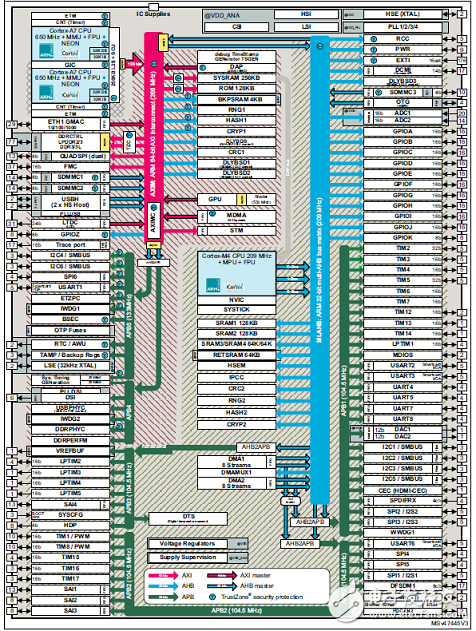
图1.STM32MP157C框图
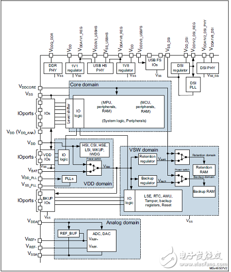
图2.STM32MP157C电源方案图
评估板STM32MP157C-EV1和STM32MP157A-EV1
The STM32MP157C-EV1 and STM32MP157A-EV1 Evaluation boards are designed as complete demonstration anddevelopment platforms for STMicroelectronics Arm®-based dual -A7 32 bits and Cortex®-M4 32 bits MPUs in the STM32MP1Series. They leverage the capabilities of STM32MP1 Series microprocessors for the user to develop applications, using STM32MPU OpenSTLinux Distribution software for the main processor, and STM32CubeMP1 software for the co-processor. Theyinclude an ST-LINK embedded debug tool, LEDs, push-buttons, one joystick, 1-Gbps Ethernet, CAN FD, one USB OTG Micro-AB connector, four USB Host Type-A connectors, LCD display with touch panel, camera, stereo headset jack with analogmicrophone input, four digital microphones, one SPDIF Rx/Tx, Smartcard, microSD™ card, and eMMC, NOR and NAND Flashmemories.
STM32MP157x-EV1 is used as the reference design for user application development,although it is not considered as final application.To expand the functionality of the STM32MP157C-EV1 and STM32MP157A-EV1 Evaluation boards, two GPIO expansionconnectors are also available for motor control and Raspberry Pi® shields.
An ST-LINK/V2-1 is integrated on the board, as embedded in-circuit debugger and programmer for the STM32 MPU and theUSB Virtual COM port bridge.
图3.评估板STM32MP157C-EV1外形图
图4.评估板STM32MP157x-EV1外形图:左:顶视图;右:底视图
评估板STM32MP157x-EV1主要特性:
• STM32MP157 Arm®-based dual Cortex®-A7 32 bits + Cortex®-M4 32 bits MPU in LFBGA448 package
• ST PMIC STPMIC1A
• 2 × 4-Gbit DDR3L, 16 bits, 533 MHz
• 2 × 512-Mbit Quad-SPI Flash
• 32-Gbit eMMC v5.0
• 8-Gbit SLC NAND, 8 bits, 8-bit ECC, 4-KB PS
• 1-Gbit/s Ethernet (RGMII) compliant with IEEE-802.3ab
• USB Host 4-port hub
• USB OTG HS
• CAN FD
• 5.5“ TFT 720×1280 pixels with LED backlight, MIPI DSISM interface, and capacitive touch panel
• SAI audio codec
• 5-megapixel, 8-bit camera
• 4 × ST-MEMS digital microphones
• Smartcard
• microSD™ card
• 2 user LEDs
• 2 user and reset push-buttons, 1 wake-up button
• 4-direction joystick with selection button
• 5 V / 4 A power supply
• Board connectors:
– Ethernet RJ45
– 4 × USB Host Type-A
– USB OTG Micro-AB
– SPDIF RCA input and output
– CAN FD
– Stereo headset jack including analog microphone input
– Audio jack for external speakers
– Motor control
– External I2C
– LTDC
– Trace, JTAG, RS-232
– GPIO expansion connector (Raspberry Pi® shields capability)
– MEMS-microphone daughterboard expansion connector
• On-board ST-LINK/V2-1 debugger/programmer with USB re-enumeration capability: Virtual COM port anddebug port
• STM32CubeMP1 and full mainline open-source Linux® STM32 MPU OpenSTLinux distribution (such asSTM32MP1Starter) software and examples
• Support of a wide choice of Integrated Development Environments (IDEs) including IAR™, Keil®, GCCbasedIDEs
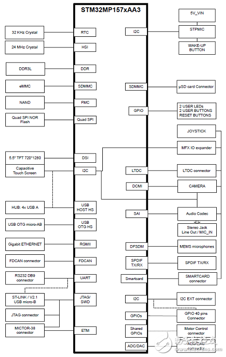
图6.评估板STM32MP157x-EV1硬件框图
评估板STM32MP157x-EV1包括:
MB1262母板
MB1262子板
MB1230 DSI(MIPI (R)标准)720p显示
MB1379子板照相机
MicroSD卡
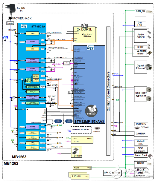
图7.评估板STM32MP157x-EV1平台电源树图
en.MB1230-C_schematic
MB1230: 1280 x 720p DSI Rocktech LCD
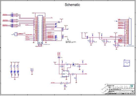
图8.MB1230-C电路图
en.MB1262-C01_schematic
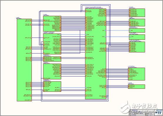
图9.MB1262-C01电路图(1)
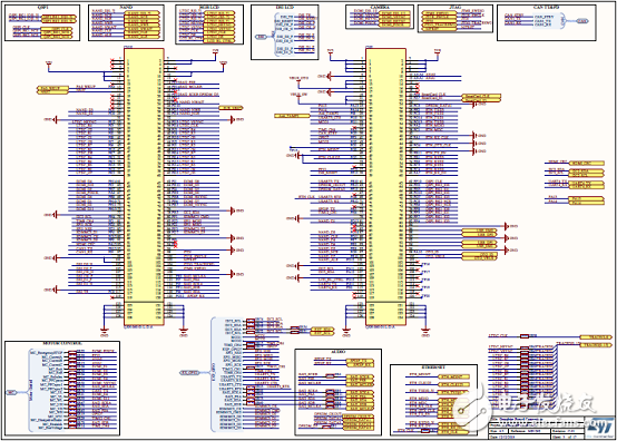
图10.MB1262-C01电路图(2)
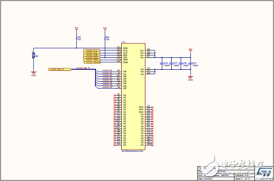
图11.MB1262-C01电路图(3)
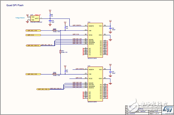
图12.MB1262-C01电路图(4)
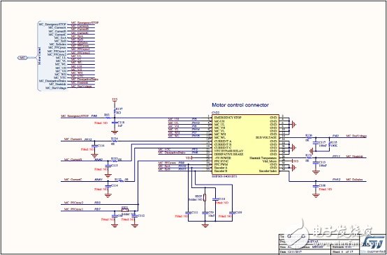
图13.MB1262-C01电路图(5)
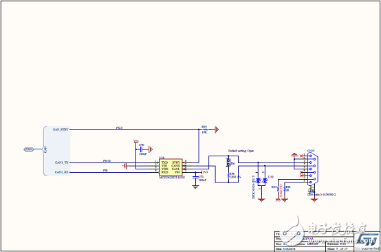
图14.MB1262-C01电路图(6)
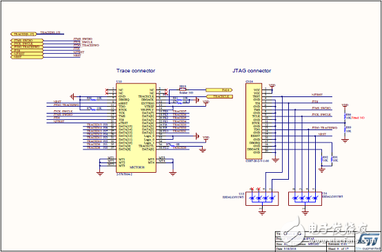
图15.MB1262-C01电路图(7)
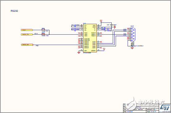
图16.MB1262-C01电路图(8)
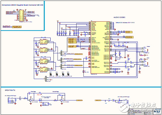
图17.MB1262-C01电路图(9)
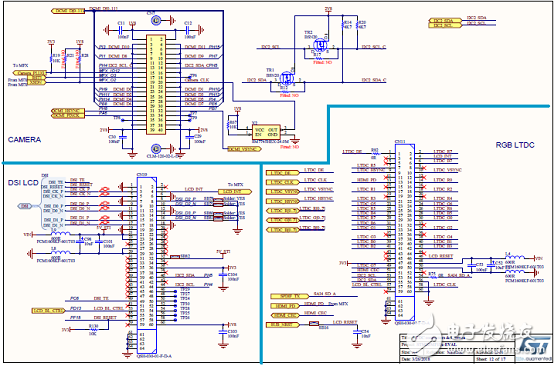
图18.MB1262-C01电路图(10)
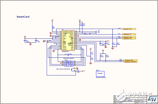
图19.MB1262-C01电路图(11)
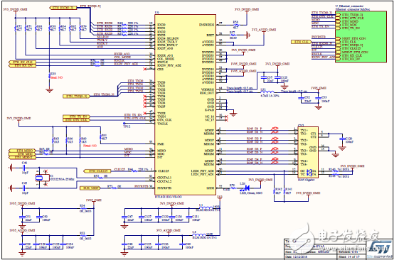
图20.MB1262-C01电路图(12)
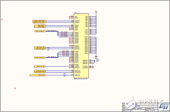
图21.MB1262-C01电路图(13)
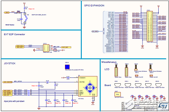
图22.MB1262-C01电路图(14)
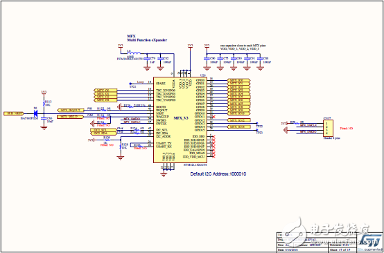
图23.MB1262-C01电路图(15)
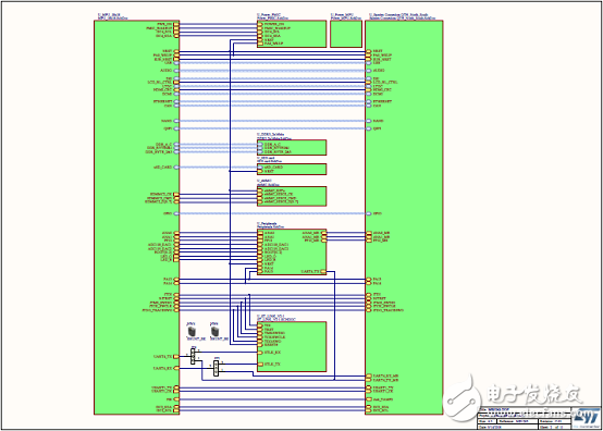
图24.MB1263-C01电路图(1)
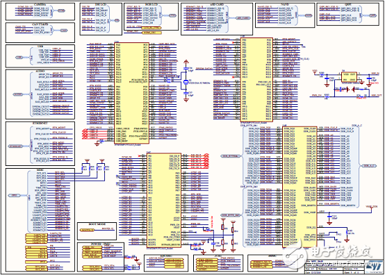
图25.MB1263-C01电路图(2)
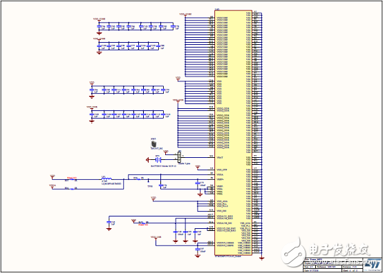
图26.MB1263-C01电路图(3)
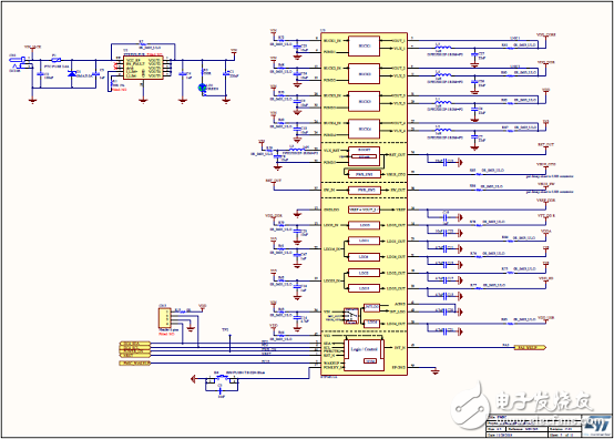
图27.MB1263-C01电路图(4)
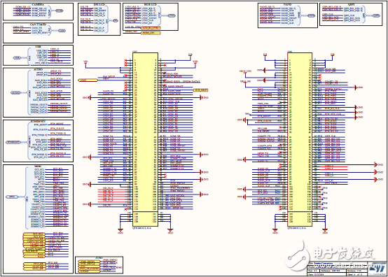
图28.MB1263-C01电路图(5)
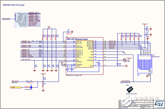
图29.MB1263-C01电路图(6)
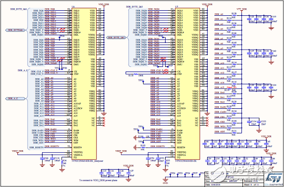
图30.MB1263-C01电路图(7)
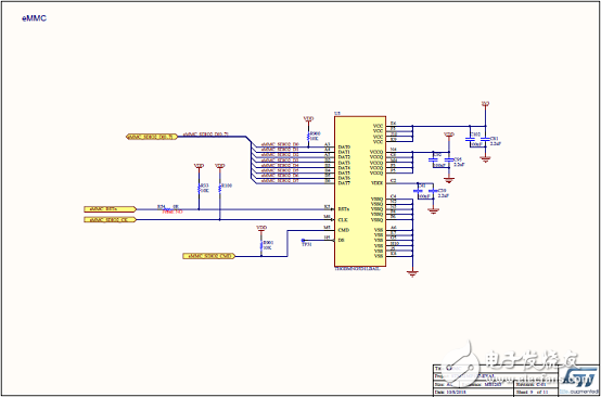
图31.MB1263-C01电路图(8)
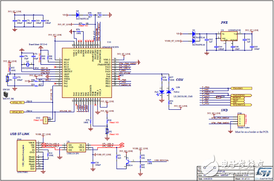
图32.MB1263-C01电路图(9)
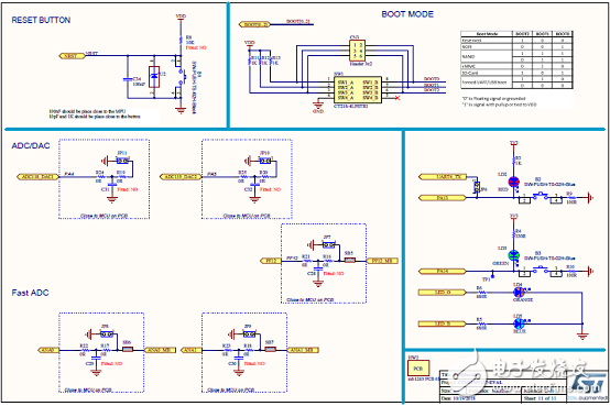
图33.MB1263-C01电路图(10)
en.MB1379-A01_schematic
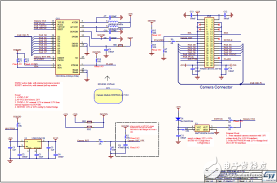
图34.MB1379-A01电路图
图35.MB1379-A01 PCB外形图
-
MPU
+关注
关注
0文章
293浏览量
48352 -
ST公司
+关注
关注
1文章
45浏览量
31524
发布评论请先 登录
相关推荐
如何在STM32MP157C DK2上实现管脚输出PTP的PPS信号?
怎么看ST公司Linux MPU第一款芯片STM32MP157?
【100ASK_STM32MP157(带屏)试用体验】开箱贴,太赞了(1)
stm32mp157开发的相关资料分享
STM32MP157C如何从eMMC启动?
STM32MP1部件号具有像STM32MP157C/F这样的安全引导选项吗?
无法在odyssey Stm32mp157c板上使用GPU咋办呢
意法半导体STM32MP157A MPU加持,米尔科技首款ST Linux开发板MYD-YA157C评测
【视频】华清远见stm32mp157开发入门指导(7讲)

意法半导体STM32MP157A MPU加持,米尔科技首款ST Linux开发板MYD-YA157C评测


 工商网监
工商网监
评论