 基于Cypress PSoC 63 MCU系列开发方案
Cypress公司的PSoC 63MCU系列是集成了Arm® Cortex™ CPU(单核和多核)的可升级和可配置的可编嵌入系统控制器,采用超低功耗40nm平台,包括有低功耗闪存和数字可编逻辑的双核微控制器(150-MHz Arm Cortex-M4F CPU和100-MHz Cortex M0+ CPU),高性能模数和数模转换器,低功耗比较器以及标准通信和定时外设,并提供BLE 5.0兼容的无线连接,可开发各种创新型物联网应用.主要用在可穿戴设备,个人医疗设备和无线音箱等.本文介绍了PSoC 63MCU系列主要特性,框图,以及评估板CY8CKIT-062-BLE主要特性,框图和电路图.
PSoC® is a scalable and reconfigurable platform architecture for a family of
programmable embedded system controllers withArm® Cortex™ CPUs (single and multi-core). The PSoC 63 product family, based on an ultra low-power 40-nm platform, is a combinationof a dual-core microcontroller with low-power Flash technology and digital programmable logic, high-performanceanalog-to-digital and digital-to-analog conversion, low-power comparators, and standard communication and timing peripherals. ThePSoC 63 family provides wireless connectivity with BLE 5.0 compliance.
PSoC 63MCU系列主要特性:
32-bit Dual Core CPU Subsystem
■ 150-MHz Arm Cortex-M4F CPU with single-cycle multiply(Floating Point and Memory Protection Unit)
■ 100-MHz Cortex M0+ CPU with single-cycle multiply and MPU.
■ User-selectable core logic operation at either 1.1 V or 0.9 V
■ Inter-processor communication supported in hardware
■ 8 KB 4-way set-associative Instruction Caches for the M4 andM0+ CPUs respectively
■ Active CPU power consumption slope with 1.1-V core operationfor the Cortex M4 is 40 μA/MHz and 20 μA/MHz for the CortexM0+, both at 3.3-V chip supply voltage with the internal buckregulator
■ Active CPU power consumption slope with 0.9-V core operationfor the Cortex M4 is 22 μA/MHz and 15 μA/MHz for the CortexM0+, both at 3.3-V chip supply voltage with the internal buckregulator
■ Two DMA controllers with 16 channels each
Flash Memory Sub-system
■ 1 MB Application Flash with 32-KB EEPROM area and 32-KBSecure Flash
■ 128-bit wide Flash accesses reduce power
■ SRAM with Selectable Retention Granularity
■ 288-KB integrated SRAM
■ 32-KB retention boundaries (can retain 32 KB to 288 KB in32-KB increments)
■ One-Time-Programmable (OTP) E-Fuse memory for validationand security
Bluetooth Low Energy (Bluetooth Smart) BT 5.0Subsystem
■ 2.4-GHz RF transceiver with 50-ohmantenna drive
■ Digital PHY
■ Link Layer engine supporting master and slave modes
■ Programmable output power: up to 4 dBm
■ RX sensitivity: –95 dBm
■ RSSI: 4-dB resolution
■ 5.7 mA TX (0 dBm) and 6.7 mA RX (2 Mbps) current with 3.3-Vbattery and internal SIMO Buck converter
■ Link Layer engine supports four connections simultaneously
■ Supports 2 Mbps LE data rate
Low-Power 1.7-V to 3.6-V Operation
■ Active, Low-power Active, Sleep, Low-power Sleep, DeepSleep, and Hibernate modes for fine-grained powermanagement
■ Deep Sleep mode current with 64-KB SRAM retention is 7 μAwith 3.3-V external supply and internal buck
■ On-chip Single-In Multiple Out (SIMO) DC-DC Buck converter,<1 μA quiescent current
■ Backup domain with 64 bytes of memory and Real-Time-Clock
Flexible Clocking Options
■ On-chip crystal oscillators (High-speed, 4 to 33 MHz, andWatch crystal, 32 kHz)
■ Phase Locked Loop (PLL) for multiplying clock frequencies
■ 8 MHz Internal Main Oscillator (IMO) with ±2% accuracy
■ Ultra low-power 32 kHz Internal Low-speed Oscillator (ILO)with ±10% accuracy
■ frequency Locked Loop (FLL) for multiplying IMO frequency
Serial Communication
■ Nine independent run-time reconfigurable serial communicationblocks (SCBs), each is software configurable as I2C,SPI, or UART
Timing and Pulse-Width Modulation
■ Thirty-two Timer/Counter Pulse-Width Modulator (TCPWM)blocks
■ Center-aligned, Edge, and Pseudo-random modes
■ Comparator-based triggering of Kill signals
Up to 78 Programmable GPIOs
■ Drive modes, strengths, and slew rates are programmable
■ Six overvoltage tolerant (OVT) pins
Packages
■ 116-BGA and 104-MCSP packages with PSoC 6 and BLERadio
Audio Subsystem
■ I2S Interface; up to 192 kilosamples (ksps) Word Clock
■ Two PDM channels for stereo digital microphones
QSPI Interface
■ Execute-In-Place (XIP) from external Quad SPI Flash
■ On-the-fly encryption and decryption
■ 4-KB QSPI cache for greater XIP performance with lower power
■ Supports 1, 2, 4, and Dual-Quad interfaces
Programmable Analog
■ 12-bit 1 Msps SAR ADC with differential and single-endedmodes and Sequencer with signal averaging
■ One 12-bit voltage mode DAC with < 5-μs settling time
■ Two opamps with low-power operation modes
■ Two low-power comparators that operate in Deep Sleep andHibernate modes.
■ Built-in temp sensor connected to ADC
Programmable Digital
■ 12 programmable logic blocks, each with 8 Macrocells and an8-bit data path (called universal digital blocks or UDBs)
■ Usable as drag-and-drop Boolean primitives (gates, registers),or as Verilog programmable blocks
■ Cypress-provided peripheral component library using UDBs toimplement functions such as Communication peripherals (forexample, LIN, UART, SPI, I2C, S/PDIF and other protocols),Waveform Generators, Pseudo-Random Sequence (PRS)generation, and many other functions.
■ Smart I/O (Programmable I/O) blocks enable Booleanoperations on signals coming from, and going to, GPIO pins
■ Two ports with Smart_IO blocks, capability are provided; theseare available during Deep Sleep
Capacitive Sensing
■ Cypress Capacitive Sigma-Delta (CSD) provides best-in-classSNR, liquid tolerance, and proximity sensing
■ Mutual Capacitance sensing (Cypress CSX) with dynamicusage of both Self and utual sensing
■ Wake on Touch with very low current
■ Cypress-supplied software component makes capacitivesensing design fast and easy
■ Automatic hardware tuning (SmartSense™)
Energy Profiler
■ Block that provides history of time spent in different powermodes
■ Allows software energy profiling to observe and optimizeenergy consumption
PSoC Creator Design Environment
■ Integrated Development Environment provides schematicdesign entry and build (with analog and digital automaticrouting) and code development and debugging
■ Applications Programming Interface (API Component) for allfixed-function and programmable peripherals
■ Bluetooth Smart Component (BLE4.2 compliant protocol stack)with Application level function calls and Profiles
Industry-Standard Tool Compatibility
■ After schematic entry, development can be done withArm-based industry-standard development tools
■ Configure in PSoC Creator and export to Arm/Keil or IAR IDEsfor code development and debugging
■ Supports industry standard Arm Trace Emulation Trace Module
Security Built into Platform Architecture
■ Multi-faceted secure architecture based on ROM-based root oftrust
■ Secure Boot uninterruptible until system protection attributesare established
■ Authentication during boot using hardware hashing
■ Step-wise authentication of execution images
■ Secure execution of code in execute-only mode for protectedroutines
■ All Debug and Test ingress paths can be disabled
Cryptography Accelerators
■ Hardware acceleration for Symmetric and Asymmetriccryptographic methods (AES, 3DES, RSA, and ECC) and Hashfunctions (SHA-512, SHA-256)
■ True Random Number Generator (TRNG) function

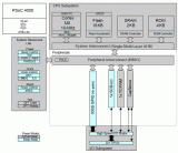
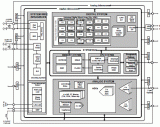
图1.PSoC 63MCU系列框图
评估板CY8CKIT-062-BLE
Thank you for your interest in the CY8CKIT-062-BLE PSoC 6 BLE Pioneer Kit. The PSoC 6 BLEPioneer Kit enables you to evaluate and develop your applications using the PSoC 6 MCU withBluetooth Low Energy (BLE) Connectivity (hereafter called “PSoC 6 MCU”).
PSoC 6 MCU is Cypress’ latest, ultra-low-power PSoC specifically designed for wearables and IoTproducts. PSoC 6 MCU is a true programmable embedded system-on-chip, integrating a 150-MHzARM® Cortex®-M4 as the primary application processor, a 100-MHz ARM Cortex®-M0+ thatsupports low-power operations, up to 1 MB Flash and 288 KB SRAM, an integrated BLE 4.2 radio,CapSense® touch-sensing, and programmable analog and digital peripherals that allow higherflexibility, in-field tuning of the design, and faster time-to-market.
The PSoC 6 BLE Pioneer board offers compatibility with Arduino™ shields. The board features aPSoC 6 MCU, a 512-Mb NOR flash, onboard programmer/debugger (KitProg2), USB Type-C powerdelivery system (EZ-PD™ CCG3), 5-segment CapSense slider, two CapSense buttons, one Cap-Sense proximity sensing header, an RGB LED, two user LEDs, and one push button. The boardsupports operating voltages from 1.8 V to 3.3 V for PSoC 6 MCU.
The CY8CKIT-062-BLE package includes a CY8CKIT-028-EPD E-INK Display Shield that containsa 2.7-inch E-INK display, a motion sensor, a thermistor, and a PDM microphone. The kit packagealso contains a CY5677 CySmart BLE 4.2 USB Dongle that is factory-programmed to emulate a BLEGAP Central device, enabling you to emulate a BLE host on your computer.
You can use PSoC Creator™ to develop and debug your PSoC 6 MCU projects. PSoC Creator isCypress’ standard integrated design environment (IDE). PSoC Creator also supports exporting yourdesigns to other third party firmware development tools.
If you are new to PSoC 6 MCU and PSoC Creator IDE, you can find introductions in the applicationnote AN210781 - Getting Started with PSoC 6 MCU with Bluetooth Low Energy (BLE) Connectivity.
The CY8CKIT-062-BLE package has the following contents.
■ PSoC 6 BLE Pioneer Board
■ CY8CKIT-028-EPD E-INK Display Shield
■ CY5677 CySmart BLE 4.2 USB Dongle
■ USB Type-A to Type-C cable
■ Four jumper wires (4 inches each)
■ Two proximity sensor wires (5 inches each)
■ Quick Start Guide
图2. 评估板CY8CKIT-062-BLE组图外形图
评估板CY8CKIT-062-BLE主要特性:
■ PSoC 6 MCU with BLE connectivity
■ Expansion headers that are compatible with Arduino Uno™ 3.3 V shields1 and Digilent® Pmod™modules
■ 512-Mbit external quad-SPI NOR Flash that provides a fast, expandable memory for data andcode
■ KitProg2 onboard programmer/debugger with mass storage programming, USB to UART/I2C/SPI bridge functionality, and custom applications support
■ EZ-PD CCG3 USB Type-C power delivery (PD) system with rechargeable lithium-ion polymer (Li-Po) battery support2
■ CapSense touch-sensing slider (5 elements), two buttons, all of which are capable of both selfcapacitance(CSD) and mutual-capacitance (CSX) operation, and a CSD proximity sensor that letyou evaluate Cypress’ fourth-generation CapSense technology
■ 1.8 V to 3.3 V operation of PSoC 6 MCU is supported. An additional 330 mF super-capacitor isprovided for backup domain supply (Vbackup)
■ Two user LEDs, a RGB LED, a user button, and a reset button for PSoC 6 MCU. Two buttons andthree LEDs for KitProg2
图3.评估板PSoC 6 BLE Pioneer板外形图(正面)
评估板PSoC 6 BLE Pioneer板中数字内容为:
图4.评估板PSoC 6 BLE Pioneer板框图
图5.评估板PSoC 6 BLE Pioneer板电路图(1)

图6.评估板PSoC 6 BLE Pioneer板电路图(2)

图7.评估板PSoC 6 BLE Pioneer板电路图(3)

图8.评估板PSoC 6 BLE Pioneer板电路图(4)

图9.评估板PSoC 6 BLE Pioneer板电路图(5)

图10.评估板PSoC 6 BLE Pioneer板电路图(6)

图11.评估板PSoC 6 BLE Pioneer板电路图(7)

图12.评估板PSoC 6 BLE Pioneer板电路图(8)

图13.评估板PSoC 6 BLE Pioneer板电路图(9)

图14.评估板PSoC 6 BLE Pioneer板电路图(10)
图15.评估板PSoC 6 BLE Pioneer板电路图(11)

图16.评估板PSoC 6 BLE Pioneer板电路图(12)
-
PSoC
+关注
关注
12文章
167浏览量
91097 -
Cypress
+关注
关注
10文章
136浏览量
81524
发布评论请先 登录
相关推荐
Cypress推出PSoC 5LP器件,助力高精度模拟应用
Cypress PSoC蓝牙低功耗开发方案与电路图详解
深入测试:大道至简—Cypress PSoC 4000S CapSense原型开发套件评测(二)
Cypress PSoC 4000S CapSense原型开发套件
e络盟推出 Cypress PSoC 6 BLE 先锋套件:开发提供高性能、低功耗且可实现最大安全性的下一代物联网设计
Cypress semiconductor 的CY7C63xxx USB微控制器系列的固件讨论
Cypress PSoC蓝牙低功耗开发设计攻略
cypress的PSoC的开发板有多少种类型?在哪里可以买到cypress的PSoC的开发板?
赛普拉斯Cypress PSoC 6 MCU简介及常见4款开发套件工具板
PSoC Creator IDE的编译器是cypress与K
Mouser备货Cypress PSoC 4可编程SoC
Cypress的PSoC系列产品CY8C22x45_CY8C21345数据手册免费下载
cypress公司的PSoC 4000Pioneer开发板方案介绍
全新的PSoC 6 MCU专为物联网设备而设计
Cypress PSoC®5开发板特性_电路图及PCB元件布局图


 工商网监
工商网监
评论