 基于RSL10超低功耗多协议蓝牙5系统级芯片解决方案
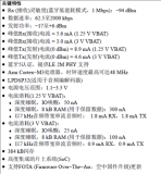
On Semi公司的RSL10超低功耗多协议蓝牙5系统级芯片(SoC),采用1.2V和1.5V电池工作,支持工作电压在1.1V和3.3V之间;器件具有双核架构和2.4GHz收发器,深睡眠模式功耗62.5nW,接收模式Rx功耗为7mW,接收灵敏度-94 dBm,发送功率-17 dBm到 +6 dBm.器件还集成了高效功率管理单元,振荡器,闪存,RAM,DMA控制器,外设和接口。主要用在超低功耗IoT超低功耗连接,以及心率监视器等。本文介绍了RSL10主要特性,框图和架构图,降压模式和LDO模式应用框图以及评估板EVBUM2529/D主要特性,电路图和材料清单。
ON Semiconductor’s RSL10 is a multiprotocol Bluetooth 5 certified radio SoC, which brings ultra-low-power wireless technology to IoT. Offering the industry’s lowest power consumption, RSL10 helps provide devices like heart rate monitors with advanced wireless features while optimizing system size and battery life.
Unlike most other multi-protocol radio SoCs, RSL10 is specifically designed for applications using 1.2 V and 1.5 V batteries, and supports a voltage supply range between 1.1 V and 3.3 V without a required DC/DC converter. The highly-integrated radio SoC features a dual-core architecture and a 2.4 GHz transceiver, providing the flexibility to support Bluetooth low energy technology and 2.4 GHz proprietary or custom protocols.
RSL10主要特性:
Ultra-low-power: RSL10 provides an incredibly power efficient operation for a wide range of applications with its superior overall power profile, including some of the industry’s best numbers in deep sleep Mode (62.5 nW) and Rx in receive mode (7 mW)
Advanced multi-protocol wireless functionality:
Rx sensitivity: -94 dBm
Transmitting power: -17 dBm to +6 dBm
Supports Bluetooth low energy (BLE) and 2.4 GHz proprietary/custom protocols
Supports firmware over the air (FOTA)
Flexible voltage supply range (1.1 V and 3.3 V): Supports devices using 1.2 V and 1.5 V batteries without a required external DC/DC converter
Ultra-miniature: RSL10 is offered in a 5.50 mm2 WLCSP and a 6 mm x 6 mm QFN. For added miniaturization, the radio SoC can be integrated into System-in-Package (SiP) solutions which combine RSL10 with a custom ASIC
Sophisticated dual-core architecture: Features a programmable ARM® Cortex®-M3 processor for clocking speeds up to 48 MHz and the flexibility to support 2.4 GHz proprietary and custom protocol stacks. An embedded digital signal processor (DSP) enables signal processing intensive applications, such as wireless audio codecs
On-chip and software wireless support: Features a 2.4 GHz padio frequency front-end (RFFE) and a Bluetooth 5 certified baseband controller which supports 2 Mbps data rates. A wide range of supported BLE protocols are provided in the RSL10 development tools kit
Highly-integrated system-on-chip (SoC): The powerful dual-core architecture is complemented by high-efficiency power management units, oscillators, Flash, and RAM memories, a DMA controller, and peripherals and interfaces
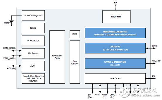
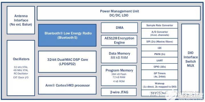
图1.RSL10框图
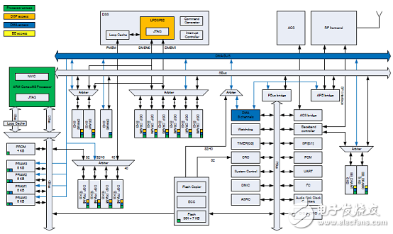
图2.RSL10架构图
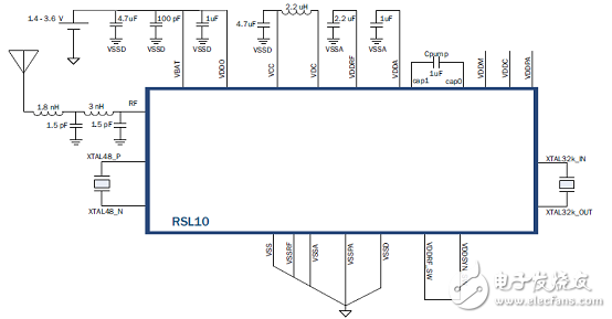
图3.RSL10降压模式应用框图
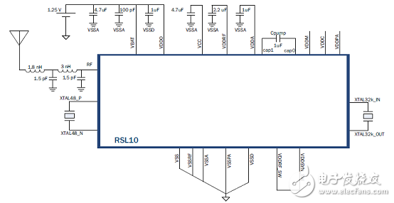
图4.RSL10 LDO模式应用框图
评估板EVBUM2529/D
The RSL10 development board is used to easily develop Bluetooth® low energy technology-enabled applications based on the industry’s lowest power radio System-on-Chip (SoC)。
The RSL10 Evaluation and Development Board is usedfor evaluating the RSL10 SoC and for applicationdevelopment. The board provides access to all input andoutput connections via 0.1″ standard headers. The on-boardcommunication interface circuit provides communication tothe board from a host PC. The communication interfacetranslates RSL10 SWJ−DP debug port signals to the USB ofthe host PC. There is also an on-board 4-bit level shifter fordebugging; it translates the I/O signal level of RSL10 to the 3.3 V digital logic level. It is not enabled by default; youenable it when it is needed.
图5.评估板EVBUM2529/D外形图
The Evaluation and Development Board enablesdevelopers to evaluate the performance and capabilities ofthe RSL10 radio SoC in addition to developing,demonstrating and debugging applications.
评估板EVBUM2529/D主要特性:
• J−Link onboard solution provides a SWJ−DP(serial-wire and/or JTAG) interface that enables you todebug the board via a USB connection with the PC
• Alternate onboard SWJ−DP (serial-wire and/or JTAG)interface for ArmR CortexR−M3 processor debugging
• Access to all RSL10 peripherals via standard 0.1″headers
• Onboard 4-bit level translator to translate the LPDSP32debug interface at low voltage to a 3.3 V JTAGdebugger
• Antenna matching and filtering network
• Integrated PCB antenna
In addition, the QFN board provides:
• Compliance with the Arduino form factor
• Support for PMOD (i.e., J4 is a standard connector)
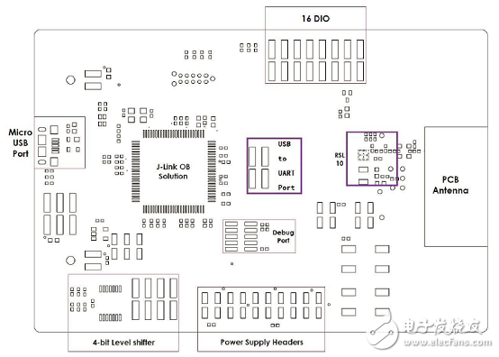
图6. WLCSP评估板电路位置图
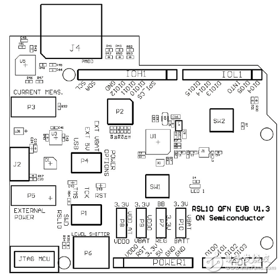
图7. QFN评估板电路位置图(顶视图)
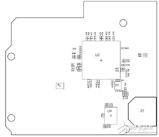
图8. QFN评估板电路位置图(底视图)
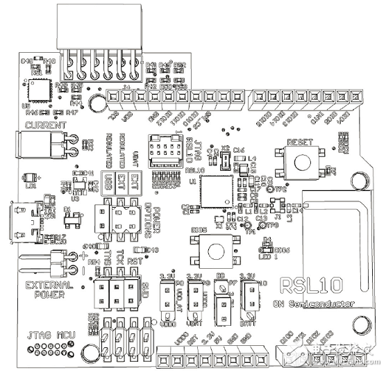
图9. QFN评估板三维线路位置图(顶视图)
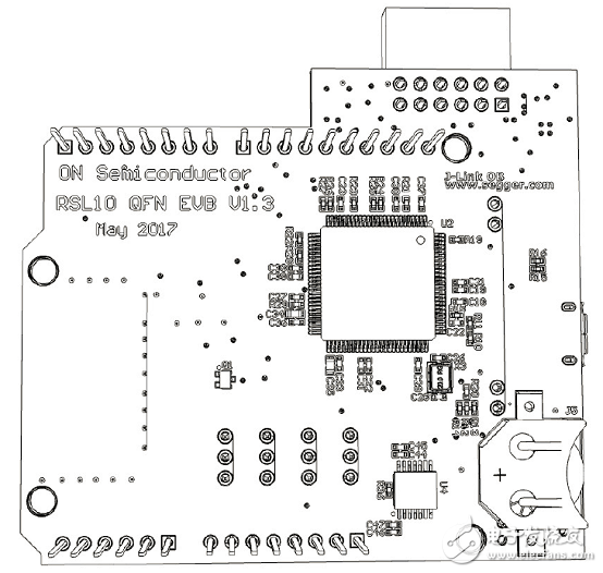
图10. QFN评估板三维线路位置图(底视图)
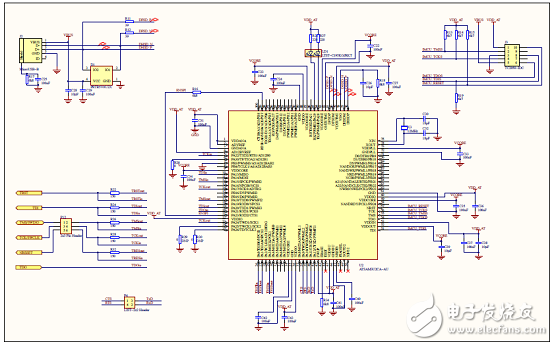
图11. 评估板EVBUM2529/D电路图:MCU接口
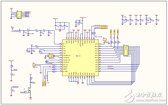
图12. 评估板EVBUM2529/D电路图:RSL10
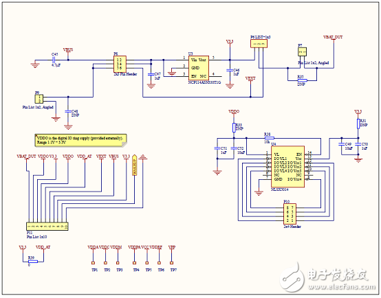
图13. 评估板EVBUM2529/D电路图:电源
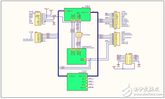
图14. 评估板EVBUM2529/D电路图:顶级(Arduino接口)
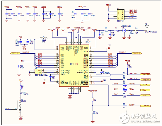
图15. 评估板EVBUM2529/D电路图:RSL10 SoC
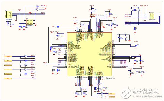
图16. 评估板EVBUM2529/D电路图:MCU接口
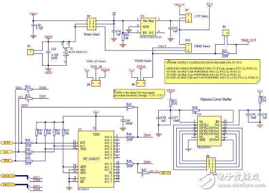
图17. 评估板EVBUM2529/D电路图:电源
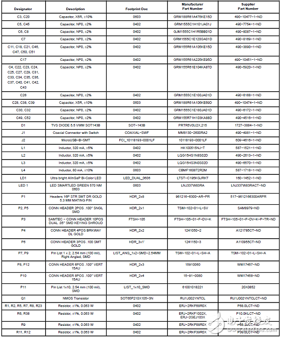
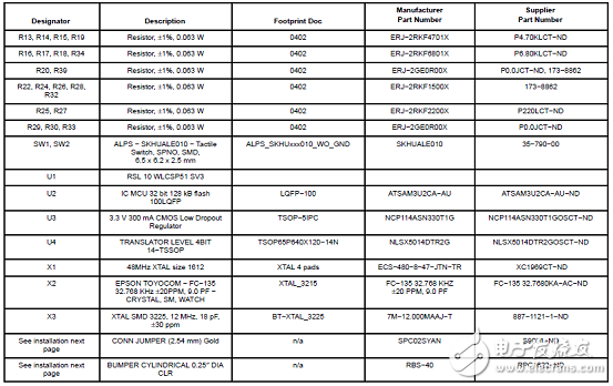
RSL10 WLCSP评估板V1.2材料清单:
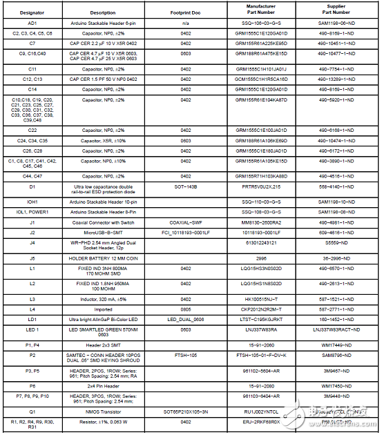
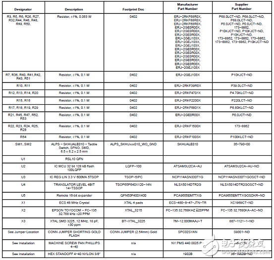
RSL10 QFN评估板V1.3材料清单:
-
振荡器
+关注
关注
28文章
3507浏览量
137608 -
蓝牙5
+关注
关注
21文章
50浏览量
109062
发布评论请先 登录
相关推荐
安森美最热门产品RSL10无线电SoC和KAF-09001 CCD图像传感器EDN
更易于设计导入的蓝牙低功耗技术
RSL10传感器开发套件怎么助力物联网?
【大联大世平ON Semiconductor BLE5.0 RSL10开发板试用申请】基于世平ON Semiconductor BLE5.0 RSL10开发板智能可穿戴设备研发
【大联大世平ON Semiconductor BLE5.0 RSL10开发板试用申请】基于RSL10的智能门锁
【大联大世平ON Semiconductor BLE5.0 RSL10开发板试用体验】板子牛刀小试(一)
【大联大世平ON Semiconductor BLE5.0 RSL10开发板试用体验】虽然小,但很强 --记安森美RSL10
实现超低功耗蓝牙控制的可调光智能照明方案的方法
基于Kemet PL-N823-01和OnSemi RSL10蓝牙低功耗SoC
贸泽电子备货RSL10 多协议片上系统,为各应用提供超低功耗无线连接
On Semi RSL10蓝牙5多协议无线片上系统(S0C)开发方案


 工商网监
工商网监
评论