 Microchip PIC18(L)F25xx83系列MCU CAN应用开发方案
Microchip公司的PIC18(L)F25xx83系列是具有CAN技术的低功耗高性能微控制器(MCU),系列产品中具有多种通信外设如CAN,SPI,两个I2C,两个UART,LIN,DMX和DALI,可以处理智能应用的多种有线和无线通信协议。系统的核采用C汇编优化RISC架构,工作速度高达64MHz,指令周期62.5ns,有两个直接内存存取(DMA)控制器,主要用在汽车电子,工业应用和医疗电子市场。本文介绍了PIC18(L)FXXK83主要特性,框图以及Curiosity High Pin Count (HPC)开发板主要特性和电路图。
The PIC18(L)FXXK83 is a full-featured CAN product family that can be used in automotive and industrial applications.The multitude of communication peripherals found on the product family, such as CAN, SPI, two I2Cs, two UARTs, LIN,DMX, and DALI can handle a wide range of wired and wireless (using external modules) communication protocols forintelligent applications. This family includes a 12-bit ADC with Computation (ADC2) extensions for automated signalanalysis to reduce the complexity of the application. This, combined with the Core Independent Peripherals integrationcapabilities, enables functions for motor control, power supply, sensor, signal and user interface applications.
PIC18(L)FXXK83主要特性:
Core Features
• C Compiler Optimized RISC Architecture
• Operating Speed:
- Up to 64 MHz clock operation
- 62.5 ns minimum instruction cycle
• Two Direct Memory Access (DMA) Controllers:
- Data transfers to SFR/GPR spaces fromeither Program Flash Memory, DataEEPROM or SFR/GPR spaces
- User-programmable source and destinationsizes
- Hardware and software-triggered datatransfers
• System Bus Arbiter with User-ConfigurablePriorities for Scanner and DMA1/DMA2 with
respect to the main line and interrupt execution
• Vectored Interrupt Capability:
- Selectable high/low priority
- Fixed interrupt latency
- Programmable vector table base address
• 31-Level Deep Hardware Stack
• Low-Current Power-on Reset (POR)
• Configurable Power-up Timer (PWRT)
• Brown-Out Reset (BOR)
• Low-Power BOR (LPBOR) Option
• Windowed Watchdog Timer (WWDT):
- Variable prescaler selection
- Variable window size selection
- Configurable in hardware or software
Memory
• Up to 64 KB Flash Program Memory
• Up to 4 KB Data SRAM Memory
• Up to 1 KB Data EEPROM
• Memory Access Partition (MAP):
- Configurable boot and app region sizes withindividual write-protections
• Programmable Code Protection
• Device Information Area (DIA) stores:
- Unique IDs and Device IDs
- Temp Sensor factory-calibrated data
- Fixed Voltage Reference calibrated data
• Device Configuration Information (DCI) stores:
- Erase row size
- Number of write latches per row
- Number of user rows
- Data EEPROM memory size
- Pin count
Operating Characteristics
• Operating Voltage Range:
- 1.8V to 3.6V (PIC18LF25/26K83)
- 2.3V to 5.5V (PIC18F25/26K83)
• Temperature Range:
- Industrial: -40℃ to 85℃
- Extended: -40℃ to 125℃
Power-Saving Functionality
• DOZE mode: Ability to run CPU core slower thanthe system clock
• IDLE mode: Ability to halt CPU core while internalperipherals continue operating
• SLEEP mode: Lowest power consumption
• Peripheral Module Disable (PMD):
- Ability to disable unused peripherals tominimize power consumption
eXtreme Low-Power (XLP) Features
• Sleep mode: 60 nA @ 1.8V, typical
• Windowed Watchdog Timer: 720 nA @ 1.8V,typical
• Secondary Oscillator: 580 nA @ 32 kHz
• Operating Current:
- 4 uA @ 32 kHz, 1.8V, typical
- 45 uA/MHz @ 1.8V, typical
Digital Peripherals
• Three 8-Bit Timers (TMR2/4/6) with HardwareLimit Timer (HLT):
- Hardware monitoring and Fault detection
• Four 16-Bit Timers (TMR0/1/3/5)
• Four Configurable Logic Cell (CLC):
- Integrated combinational and sequential logic
• Three Complementary Waveform Generators(CWGs):
- Rising and falling edge dead-band control
- Full-bridge, half-bridge, 1-channel drive
- Multiple signal sources
- Programmable dead band
- Fault-shutdown input
• Four Capture/Compare/PWM (CCP) modules
• Four 10-bit Pulse-Width Modulators (PWMs)
• Numerically Controlled Oscillator (NCO):
- Generates true linear frequency control
- High resolution using 20-bit accumulator and20-bit increment values
• DSM: Data Signal Modulator:
- Multiplex two carrier clocks, with glitch preventionfeature
- Multiple sources for each carrier
• Programmable CRC with Memory Scan:
- Reliable data/program memory monitoring forfail-safe operation(e.g.,ClassB)
- Calculate CRC over any portion of programmemory
• Two UART Modules:
- Modules are Asynchronous, RS-232, RS-485compatibility.
- One of the UART modules supports LINMaster and Slave, DMX mode, DALI Gearand Device protocols
- Automatic and user-timed BREAK periodgeneration
- DMA Compatible
- Automatic checksums
- Programmable 1, 1.5, and two Stop bits
- Wake-up on BREAK reception
• One SPI module:
- Configurable length bytes
- Configurable length data packets
- Receive-without-transmit option
- Transmit-without-receive option
- Transfer byte counter
- Separate Transmit and Receive Buffers with2-byte FIFO and DMA capabilities
• CAN module:
- Conforms to CAN 2.0B Active Specification
- Three operating modes: Legacy (compatiblewith existing PIC18CXX8/FXX8 CAN modules),Enhanced mode, and FIFO mode.
- Message bit rates up to 1 Mbps
- DeviceNet data byte filter support
- Six programmable receive/transmit buffers
- Three dedicated transmit buffers
- Two dedicated receive buffers
- 16 Full, 29-bit acceptance filters with dynamicassociation
- Three full, 29-bit acceptance masks
- Automatic remote frame handling
- Advanced error management features.
• Two I2C modules, SMBus, PMBus™ compatible:
- Dedicated Address, Transmit and Receivebuffers
- Bus Collision Detection with arbitration
- Bus time-out detection and handling
- Multi-Master mode
- Separate Transmit and Receive Buffers with
2-byte FIFO and DMA capabilities
- I2C, SMBus 2.0 and SMBus 3.0, and 1.8Vinput level selections
• Device I/O Port Features:
- 25 I/O pins (PIC18(L)F25K83)
- One input-only pin
- Individually programmable I/O direction,open-drain, slew rate, weak pull-up control
- Interrupt-on-change
- Three External Interrupt Pins
• Peripheral Pin Select (PPS):
- Enables pin mapping of digital I/O
• Two Signal Measurement Timer (SMT):
- 24-bit timer/counter with prescaler
Analog Peripherals
• Analog-to-Digital Converter with Computation(ADC2):
- 12-bit with up to 24 external channels
- Automated post-processing
- Automated math functions on input signals:averaging, filter calculations, oversampling
and threshold comparison
- Operates in Sleep
- Integrated charge pump for improved lowvoltageoperation
• Hardware Capacitive Voltage Divider (CVD):
- Automates touch sampling and reduces softwaresize and CPU usage when touch or
proximity sensing is required
- Adjustable sample and hold capacitor array
- Two guard ring output drives
• Temperature Sensor:
- Internal connection to ADC
- Can be calibrated for improved accuracy
• Two Comparators:
- Low-Power/High-Speed mode
- Fixed Voltage Reference at noninvertinginput(s)
- Comparator outputs externally accessible
• 5-Bit Digital-to-Analog Converter (DAC):
- 5-bit resolution, rail-to-rail
- Positive Reference Selection
- Unbuffered I/O pin output
- Internal connections to ADCs andcomparators
• Voltage Reference:
- Fixed Voltage Reference with 1.024V, 2.048Vand 4.096V output levels
Flexible Oscillator Structure
• High-Precision Internal Oscillator:
- Selectable frequency range up to 64 MHz
- ±1% at calibration (nominal)
• Low-Power Internal 32 kHz Oscillator(LFINTOSC)
• External 32 kHz Crystal Oscillator (SOCS)
• External Oscillator Block with:
- x4 PLL with external sources
- Three crystal/resonator modes up to 20 MHz
- Three external clock modes up to 20 MHz
• Fail-Safe Clock Monitor
• Oscillator Start-up Timer (OST):
- Ensures stability of crystal oscillator sources
The new family is ideal for applications using CAN in the medical, industrial and automotive markets, such as motorized surgical tables, asset tracking, ultrasound machines, automated conveyors and automotive accessories.
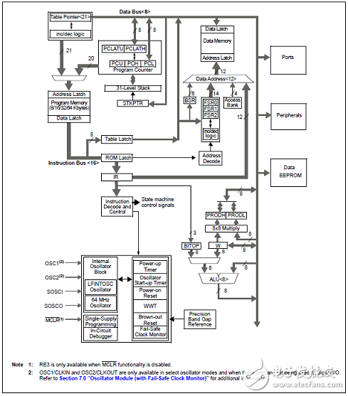
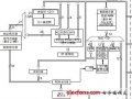
图1. PIC18(L)F25/26K83系列框图
Curiosity High Pin Count (HPC)开发板
The Curiosity High Pin Count (HPC) Development Board supports Microchip’s 28- and 40-pin 8-bit PIC® MCUs. Two unique PDIP sockets are surrounded by dual-rowexpansion headers, which allow for connectivity to all pins on the PIC MCUs.
Programming/debugging is accomplished through the PICkit™ On Board(PKOB),eliminating the need for an external programming/debugging tool. The development
board includes a set of four indication LEDs, a potentiometer, and push-button
switches. Additionally, the Curiosity HPC Board integrates two MikroElektronika
microBUS™ sockets, which accommodate a variety of plug-in Click™ Board modules
that can be used for application development.
The Curiosity High Pin Count (HPC) Development Board kit contains the following:
• Curiosity High Pin Count (HPC) Development Board
• Quick Start Guide
• PIC16F18875 MCU
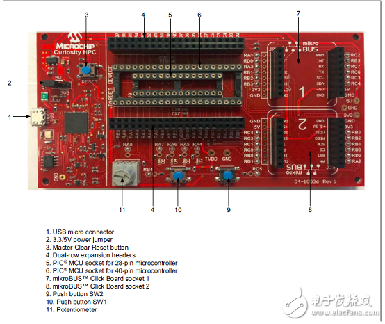
图2.Curiosity High Pin Count (HPC)开发板外形图
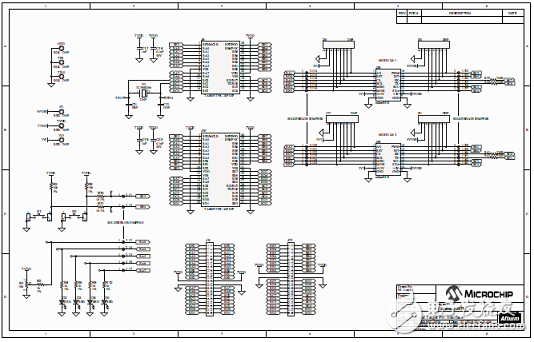
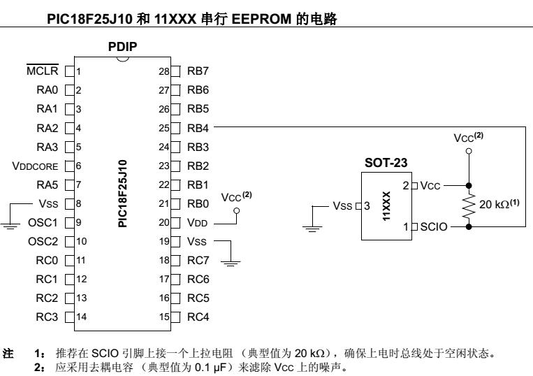
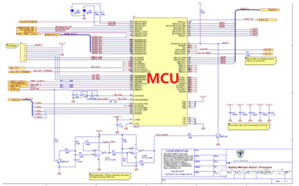
图3.Curiosity HPC开发板电路图(1)
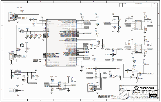
图4.Curiosity HPC开发板电路图(2)
-
microchip
+关注
关注
52文章
1455浏览量
116831 -
Mac
+关注
关注
0文章
1065浏览量
50821
发布评论请先 登录
相关推荐
MPLAB XC8 编译器microchip PIC10 12 16 18单片机开发编程工具
Microchip PIC18F46J50 8位2.4 GHz无线开发方案
【下载】《PIC项目实战:基于PIC18》
有USB与PIC18有MSD设置吗?
如何在PIC18中使用EUSART
使用C18编译器和定时器连接PIC18 MCU和兼容UNI/O®总线的串行EEPROM
贸泽电子携手Microchip带来“PIC18 Q10系列MCU介绍”直播课程
PIC18微控制器系列的数据手册免费下载
PIC18 Q10产品系列入门


 工商网监
工商网监
评论