便携式混频器电路 Portable Mixer
便携式混频器电路 Portable Mixer
Design description:
The target of this project was the design of a small portable mixer supplied by a 9V PP3 battery, keeping high quality performance.
The mixer is formed assembling three main modules that can be varied in number and/or disposition to suit everyone needs.
The three main modules are:
Input Amplifier Module: a low noise circuit equipped with a variable voltage-gain (10 - 100) pre-set, primarily intended as high quality microphone input, also suitable for low-level line input.
Tone Control Module: a three-band (Bass, Middle, Treble) tone control circuit providing unity-gain when its controls are set to flat frequency response. It can be inserted after one or more Input Amplifier Modules and/or after the Main Mixer Amplifiers.
Main Mixer Amplifier Module: a stereo circuit incorporating two virtual-earth mixers and showing the connection of one Main Fader and one Pan-Pot.
The image below shows a Block diagram of the entire mixer featuring four Input Amplifier Modules followed by four in-out switchable Tone Control Modules, one stereo Line input, four mono Main Faders, one stereo dual-ganged Main Fader, four Pan-Pots, a stereo Main Mixer Amplifier Module and two further Tone Control Modules switchable in and out for each channel, inserted before the main Left and Right outputs.
Obviously this layout can be rearranged at everyone wish.
An astonishing feature of this design lies in the fact that a complete stereo mixer as shown below in the Block diagram draws less than 6mA current!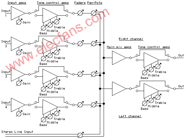
Input Amplifier Module

Parts:
R1,R2,R7_______22K 1/4W Resistors
R3,R4,R5_______47K 1/4W Resistors
R6______________4K7 1/4W Resistor
R8,R13________220R 1/4W Resistors
R9______________2K 1/2W Trimmer Cermet (See Notes)
R10___________470K 1/4W Resistor
R11___________560R 1/4W Resistor
R12___________100K 1/4W Resistor
C1____________470nF 63V Polyester Capacitor
C2,C8_________100΅F 25V Electrolytic Capacitors
C3,C4,C5________2΅2 63V Electrolytic Capacitors
C6_____________47pF 63V Ceramic Capacitor
C7______________4΅7 63V Electrolytic Capacitor
Q1____________BC560C 45V 100mA Low noise High gain PNP Transistor
Q2____________BC550C 45V 100mA Low noise High gain NPN Transistor
IC1___________TL061 Low current BIFET Op-Amp
Circuit description:
The basic arrangement of this circuit is derived from the old Quad magnetic pick-up cartridge module.
The circuit was rearranged to cope with microphone input and a single-rail low voltage supply.
This low-noise, fully symmetrical, two-transistor head amplifier layout, allows the use of a normal FET input Op-Amp as the second gain stage, even for very sensitive microphone inputs.
The voltage-gain of this amplifier can be varied by means of R9 from 10 to 100, i.e. 20 to 40dB.
Notes:
R9 can be a trimmer, a linear potentiometer or a fixed-value resistor at will.
When voltage-gain is set to 10, the amplifier can cope with 800mV peak-to-peak maximum Line levels.
Current drawing for one Input Amplifier Module is 600΅A.
Frequency response is 20Hz to 20KHz - 0.5dB.
Total Harmonic Distortion measured with voltage-gain set to 100: 2V RMS output = < 0.02% @ 1KHz; < 0.04% @ 10KHz.
Total Harmonic Distortion measured with voltage-gain set to 10 & 33: 2V RMS output = < 0.02% @ 1KHz & 10KHz.
THD is much lower @ 1V RMS output.
Maximum undistorted output voltage: 2.8V RMS.
Tone Control Module

Parts:
P1,P2_________100K Linear Potentiometers
P3____________470K Linear Potentiometer
R1,R2,R3_______12K 1/4W Resistors
R4,R5___________3K9 1/4W Resistors
R6,R7___________1K8 1/4W Resistors
R8,R9__________22K 1/4W Resistors
R10___________560R 1/4W Resistor
R11___________100K 1/4W Resistor
R12___________220R 1/4W Resistor
C1______________1΅F 63V Polyester Capacitor
C2_____________47nF 63V Polyester Capacitor
C3,C5___________4n7 63V Polyester Capacitors
C4_____________22nF 63V Polyester Capacitor
C6,C8_________100΅F 25V Electrolytic Capacitors
C7______________4΅7 63V Electrolytic Capacitor
IC1___________TL061 Low current BIFET Op-Amp
Circuit description:
This is a straightforward design using the Baxandall-type active circuitry slightly modified to obtain a three-band control. Total voltage gain of this module is 1 when controls are set in their center position.
Notes:
Current drawing for one Tone Control Module is 400΅A.
Frequency response is 20Hz to 20KHz - 0.5dB, controls flat.
Tone control frequency range: ± 15dB @ 30Hz; ± 19dB @ 1KHz; ± 16dB @ 10KHz.
Total Harmonic Distortion measured @ 2V RMS output = < 0.012% @ 1KHz; < 0.03% @ 10KHz.
THD is below 0.01% @ 1V RMS output.
Maximum undistorted output voltage: 2.5V RMS.
Main Mixer Amplifier Module

Parts:
P1,___________100K Linear Potentiometer
P2_____________10K Linear Potentiometer
R1,R2,_________15K 1/4W Resistors
R3,R4,R11,R12_100K 1/4W Resistors
R5,R6__________22K 1/4W Resistors
R7,R8_________390K 1/4W Resistors
R9,R10________560R 1/4W Resistors
R13___________220R 1/4W Resistor
C1,C2_________330nF 63V Polyester Capacitors
C3,C8_________100΅F 25V Electrolytic Capacitors
C4,C5__________10pF 63V Ceramic Capacitors
C6,C7___________4΅7 63V Electrolytic Capacitors
IC1___________TL062 Low current BIFET Dual Op-Amp
Circuit description:
The schematic of this circuit is drawn as a stereo unit to better show the input Main Fader and Pan-Pot connections. The TL062 chip contains two TL061 in the same 8 pin case and is wired as two virtual-earth mixer amplifiers having a voltage gain of about 4, to compensate for losses introduced in the passive Pan-Pot circuitry. Therefore, total voltage-gain is 1.
Each channel added to the mixer must include the following additional parts:
P1, P2, R1, R2, R3, R4, C1 and C2.
These parts must be wired as shown in the above circuit diagram, connecting R3 and R4 to pin #2 and pin #6 of IC1 for Right and Left channel respectively. These IC1 pins are the "virtual-earth mixing points" and can sum together a great number of channels.
Notes:
Current drawing for one stereo Main Mixer Amplifier Module is 800΅A.
Frequency response is 20Hz to 20KHz - 0.5dB.
Total Harmonic Distortion measured @ 2V RMS output = < 0.008% @ 1KHz; < 0.017% @ 10KHz.
THD is 0.005% @ 1V RMS output.
Maximum undistorted output voltage: 2.8V RMS.
Further Parts:
To parts listed above should be added: one Main on-off SPST switch, a LED used as pilot-light with its dropping 2K2 1/4W series-resistor, DPDT switches to enable or omit Tone Control Modules as shown in the Block diagram, input and output connectors of the type preferred, one stereo dual-gang 100K potentiometer to fade the Stereo Line Input as shown in the Block diagram, battery clip, PP3 9V battery, knobs etc.
非常好我支持^.^
(0) 0%
不好我反对
(0) 0%
相关阅读:
- [电源设计应用] 新型高线性折叠结构混频器设计 2011-03-26
- [IC应用电路图] LT5579-1.5GHz至3.8GHz高线性度上变频混频器 2010-12-10
- [模拟技术] MAX19993双通道、下变频混频器 2010-12-08
- [音响技术] MAX19997A 双通道下变频混频器 2010-10-09
- [新品快讯] 美信推出双通道、SiGe、高线性度、1200MHz至2000 2010-10-02
- [测试/封装] 有源混频器ADRF6604 2010-08-12
- [测试/封装] 2100 MHz至2600 MHz Rx混频器ADRF660 2010-08-12
- [测试/封装] 高动态范围有源混频器ADRF6655 2010-08-12
( 发表人:发烧友 )